Difference between revisions of "ANTA 64K Memory Expansion"
From CPCWiki - THE Amstrad CPC encyclopedia!
(→ROM) |
Cpcmaniaco (Talk | contribs) |
||
| (6 intermediate revisions by one other user not shown) | |||
| Line 1: | Line 1: | ||
A 64KB memory expansion by [[MHT Ingenieros]]. | A 64KB memory expansion by [[MHT Ingenieros]]. | ||
| + | |||
| + | A Spanish manufactured memory expansion intended for the Spanish market. | ||
| + | |||
| + | Originally the internal ROM is located in bank 2. | ||
| + | |||
| + | It expanded BASIC with various RSX commands (software in ROM) to allow access to the additional banks. | ||
| + | |||
| + | Features: peek and poke, Screen flipping, Printer buffer, random access to files. | ||
| + | |||
| + | The price was: 13.900 pts. | ||
| + | |||
| + | == Advert == | ||
| + | |||
| + | [[Image:ANTA64K-advert.jpg]] | ||
== Pictures == | == Pictures == | ||
<gallery> | <gallery> | ||
| + | |||
Image:Anta64K3_Top.jpg|Unit front | Image:Anta64K3_Top.jpg|Unit front | ||
Image:Anta64K3_Bottom.jpg|Unit back | Image:Anta64K3_Bottom.jpg|Unit back | ||
Image:Anta64K3_PCB_Top.jpg|PCB top | Image:Anta64K3_PCB_Top.jpg|PCB top | ||
Image:Anta64K3_PCB_Bottom.jpg|PCB bottom | Image:Anta64K3_PCB_Bottom.jpg|PCB bottom | ||
| + | |||
</gallery> | </gallery> | ||
== Technical == | == Technical == | ||
| − | * Uses port &F8F8 | + | * Uses port &F8F8 to latch data (read/write) |
| − | * | + | * Uses memory address to define where in 64KB ram to read/write. |
| − | + | ||
| − | + | ||
* NOT Dk'Tronics compatible. | * NOT Dk'Tronics compatible. | ||
* More like a ram disc | * More like a ram disc | ||
| + | |||
| + | to write: | ||
| + | |||
| + | LD BC,&F8F8 ;; ram data access | ||
| + | LD A,&34 ;; value to write | ||
| + | LD DE,&4000 ;; where in extra ram to read (0-&ffff) | ||
| + | DI | ||
| + | OUT (C),A ;; latch data for ram | ||
| + | LD A,(DE) ;; perform write into ram | ||
| + | EI | ||
| + | |||
| + | to read: | ||
| + | LD BC,&F8F8 | ||
| + | ld de,&4000 | ||
| + | di | ||
| + | in a,(c) | ||
| + | ld a,(de) ;; read value from extra ram | ||
| + | ei | ||
| + | |||
| + | each access to the I/O port must be followed by a memory read operation. | ||
| + | ROM uses single byte reads such as LD A,(DE) | ||
| + | |||
| + | * ROM has commands: | ||
| + | |||
| + | |SCREENCOPY,<ram page>,1 | ||
| + | |||
| + | copy screen at &c000 to ram page. | ||
| + | |||
| + | |||
| + | numbers can't be 0 or greater than or equal to 6. | ||
| + | |||
| + | |||
| + | PBUFF | ||
| + | NBUFF | ||
| + | PEEK | ||
| + | POKE | ||
| + | SCREENSWAP | ||
| + | BSAVE | ||
| + | BLOAD | ||
| + | CSAVE | ||
| + | CLOAD | ||
| + | OPEN | ||
| + | GET | ||
| + | CLOSE | ||
| + | PUT | ||
| + | MKILL | ||
| + | MCAT | ||
| + | MRENAME | ||
| + | FREDSK | ||
| + | RAMDSK | ||
| + | CC | ||
== ROM == | == ROM == | ||
* [[Media:MHT_Anta64k3_Rom.zip|MHT Ingenieros ANTA 64K.3 ROM]] (zipped .ROM file) | * [[Media:MHT_Anta64k3_Rom.zip|MHT Ingenieros ANTA 64K.3 ROM]] (zipped .ROM file) | ||
| + | |||
| + | [[Category:Memory expansions]] [[Category:Peripherals]] | ||
Latest revision as of 08:06, 15 November 2015
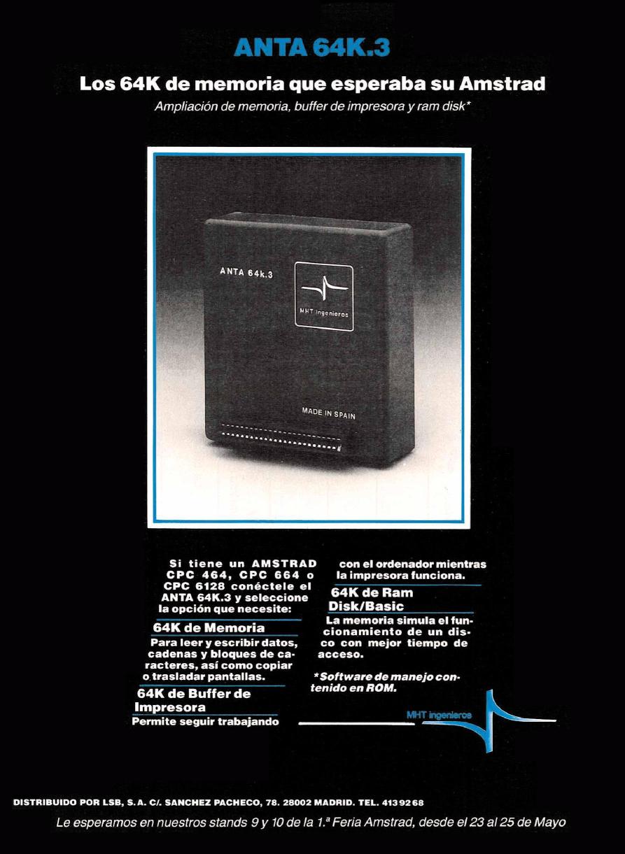
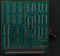
A 64KB memory expansion by MHT Ingenieros.
A Spanish manufactured memory expansion intended for the Spanish market.
Originally the internal ROM is located in bank 2.
It expanded BASIC with various RSX commands (software in ROM) to allow access to the additional banks.
Features: peek and poke, Screen flipping, Printer buffer, random access to files.
The price was: 13.900 pts.
Contents
Advert
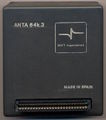
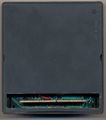
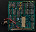
Pictures
Technical
- Uses port &F8F8 to latch data (read/write)
- Uses memory address to define where in 64KB ram to read/write.
- NOT Dk'Tronics compatible.
- More like a ram disc
to write:
LD BC,&F8F8 ;; ram data access
LD A,&34    ;; value to write
LD DE,&4000 ;; where in extra ram to read (0-&ffff)
DI
OUT (C),A   ;; latch data for ram
LD A,(DE)   ;; perform write into ram
EI
to read:
LD BC,&F8F8
ld de,&4000
di
in a,(c)
ld a,(de) ;; read value from extra ram
ei
each access to the I/O port must be followed by a memory read operation. ROM uses single byte reads such as LD A,(DE)
- ROM has commands:
|SCREENCOPY,<ram page>,1
copy screen at &c000 to ram page.
numbers can't be 0 or greater than or equal to 6.
PBUFF
NBUFF
PEEK
POKE
SCREENSWAP
BSAVE
BLOAD
CSAVE
CLOAD
OPEN
GET
CLOSE
PUT
MKILL
MCAT
MRENAME
FREDSK
RAMDSK
CC
ROM
- MHT Ingenieros ANTA 64K.3 ROM (zipped .ROM file)
