Difference between revisions of "CPC 6320 / CPC 6512 - internal 320K / 512K for CPC 6128"
| Line 19: | Line 19: | ||
[[File:CPC6320_schematics.jpg|thumbnail|none|CPC 6320 - schematics]] | [[File:CPC6320_schematics.jpg|thumbnail|none|CPC 6320 - schematics]] | ||
| + | |||
| + | |||
=== Warning / Disclaimer === | === Warning / Disclaimer === | ||
| Line 24: | Line 26: | ||
Although I have taken the utmost care preparing this documentation, I am no electronics engineer and did this only as a hobby project. I do not guarantee that it is error free and I accept no responsibility for damage to anyone’s hardware or other personal equipment or injury inflicted on you or others. | Although I have taken the utmost care preparing this documentation, I am no electronics engineer and did this only as a hobby project. I do not guarantee that it is error free and I accept no responsibility for damage to anyone’s hardware or other personal equipment or injury inflicted on you or others. | ||
| − | == Construction == | + | == Construction of the 320K (no PAL programming required) version == |
The required logic can either be built on a slim breadboard or with the help of a PCB that plugs into the PAL socket. | The required logic can either be built on a slim breadboard or with the help of a PCB that plugs into the PAL socket. | ||
| Line 122: | Line 124: | ||
<br /> | <br /> | ||
<br /> | <br /> | ||
| + | == Construction of the 320/512K (PAL programming required) version == | ||
| + | |||
| + | For a 512K version the biggest challenge is, that when we replace also the first bank we must treat the first 64K as base RAM and the other 192K as extended RAM in a way that it is properly recognised by software. | ||
| + | |||
| + | While this can be done with logic ICs it would need to much space to properly fit into a normal CPC6128. Instead this is achieved with two PAL ICs. ATF16V8 ICs are easy to find and relatively cheap but need to be programmed with e.g. an Eprom programmer like the widely available TL866-II. | ||
| + | |||
| + | What you need: | ||
| + | |||
| + | * The PCB - [https://www.cpcwiki.eu/imgs/7/70/CPC6512_Gerber.zip PCB Gerber files] | ||
| + | * 2x Pin header 1x10 | ||
| + | * 2x capacitor 100nF | ||
| + | * 2x ATF16V8 (or other PAL16L8 compatible ICs) | ||
| + | |||
| + | The assembly is pretty much identical to the PCB description above with the following changes: | ||
| + | |||
| + | * replace both RAM banks with 41256 RAM ICs | ||
| + | * connect all A8 pins on both banks so that all 16 ICs are fully parallel on all address lines. | ||
| + | * program two ATF16V8 ICs with the attached JED files and solder them to the PCB | ||
| + | * There is a connection from the PCB to D5. D5 is e.g. pin 29 on the 40007 socket. For other options check the schematics/Pinouts. | ||
| + | |||
| + | Note: It's also possible to use this PCB as a 320K version. In that case only replace the second (left) RAM bank and connect the D5 pad to GND (throughhole directly next to the D5 pad). | ||
| + | |||
| + | [[File:CPC6512 1.jpg|thumbnail|left]] [[File:CPC6512 2.jpg|thumbnail|right]] [[File:CPC6512 3.jpg|thumbnail|none]] | ||
| + | |||
== References and links == | == References and links == | ||
| − | * [https://www.cpcwiki.eu/imgs/4/40/CPC6320_Gerber.zip PCB Gerber files] | + | * [https://www.cpcwiki.eu/imgs/4/40/CPC6320_Gerber.zip PCB Gerber files - 320K version] |
| + | * [https://www.cpcwiki.eu/imgs/7/70/CPC6512_Gerber.zip PCB Gerber files - 512K version/PAL] | ||
| + | |||
* [[C't 512 KB internal RAM expansion|C't 512 KB internal RAM expansion]] | * [[C't 512 KB internal RAM expansion|C't 512 KB internal RAM expansion]] | ||
* [https://www.youtube.com/watch?v=b06CmqzrVE4 Repair video on Youtube that shows how to remove RAM ICs and add sockets] | * [https://www.youtube.com/watch?v=b06CmqzrVE4 Repair video on Youtube that shows how to remove RAM ICs and add sockets] | ||
Revision as of 10:03, 19 July 2023
Contents
A 2022s RAM expansion - straight from the mid 80s
Imagine it's spring 1987, you would have opened your favourite Amstrad magazine and a huge article says "320KB for your 6128 - DIY - dk'tronics compatible". And then it explains that cost will be in the range of just £25 / 65DM / 220Fr / 4500Pts and that all you need is a soldering iron, 3 logic ICs, a few sockets and 8 RAM ICs - all of it probably available at your local electronics store. No special skills (besides soldering) and no special equipment required.
I personally would have been fascinated and I know at least 3 people from my friends that would have instantly done that.
As we all know this never happened. RAM expansions were expensive, bulky, external pieces of hardware. The German magazine C'T published a DIY internal RAM expansion up to 512K but you had to be able to program a PAL, needed to make your own PCB and it was not compatible with dk'tronics. All you could do is, write your own programs for it. You can guess how successful it was.
But: the idea that the C'T followed was brilliant. The 41256 RAM ICs that they used could replace the 4164 chips in the 6128 out of the box. Even RAM refresh for 8 address rows was already built into the CPCs architecture. Everything is basically there. All that is missing was logic that drives the additional address line A8. And unlike the C'T it needs to be done in an easy and compatible way.
And that, it turns out, is easier than expected: By replacing the 64Kbit ICs of the second RAM bank with 256Kbit ICs (41256) and the addition of 3 standard logic ICs, the new address line A8 of these RAM ICs can be driven and a 6128 will become a 6320.
That would have been a dream in 1987.
Unlike some DIY expansions from the 80s it's still possible to do it today - all required components can still be found easily. The logic ICs are standard ICs which most "makers" probably have lying around. If not you can find them in any electronics store or on Ebay for cheap. Even if you have to source the 41256 ICs it should be possible to build this for less than 35€. To be fair, for that price you can already get an external 512KB expansion - but if you don't like this external add-ons, want to build it with your own hands and stay true to the 80s era, this expansion might be for you.
Warning / Disclaimer
Although I have taken the utmost care preparing this documentation, I am no electronics engineer and did this only as a hobby project. I do not guarantee that it is error free and I accept no responsibility for damage to anyone’s hardware or other personal equipment or injury inflicted on you or others.
Construction of the 320K (no PAL programming required) version
The required logic can either be built on a slim breadboard or with the help of a PCB that plugs into the PAL socket.
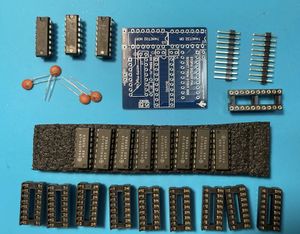
- 8x 41256 RAM IC, 150ns or faster
- 8x IC socket 16-pin (optional, but highly recommended)
- 1x 74HCT02 NOR gate
- 1x 74HCT32 OR gate
- 1x 40175 FlipFlop
- 1x IC socket, 20-pin (super flat, turned)
- 1x TriPad stripboard or PCB
- some wire
when using a TriPad stripboard:
- 2x IC socket 14-pin (optional, any will do it)
- 1x IC socket 16-pin (optional, any will do it)
- 3x capacitor 100nF
when using a PCB:
- The PCB - PCB Gerber files
- 2x Pin header 1x10
- 4x capacitor 100nF
- optional: resistor 10k, switch
With the PCB you have to solder the ICs (except for the PAL) directly to the PCB as otherwise there is not enough headroom for the keyboard.
Preparation: Replace second RAM bank
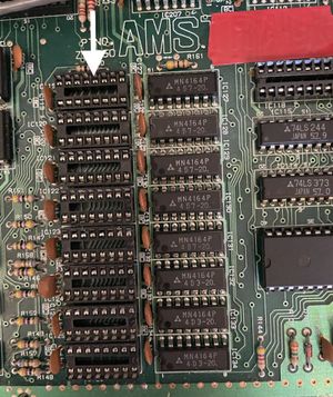
- desolder all RAM ICs of the second RAM bank (left one when looking from above). If you don't have the right tools to appropriately desolder the RAM ICs it can be easier to cut the legs and remove each leg. But of course, you will destroy the ICs with it.
- solder IC sockets into holes of the RAM ICs
- put RAM ICs into sockets
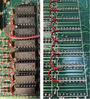
- connect pin 1 (A8) of each new IC together. Either on the backside of the motherboard or directly at pin 1 of the ICs (*)
(*) according to the schematics pin 1 should be unconnected on the motherboard. As this was different on e.g. a 464 and there are different revisions of the 6128 board it's better to check this on your motherboard. In case pin 1 is connected to GND or VCC, you have to bend up pin 1 so it's not connected to the socket and then connect pin1 of all ICs directly.
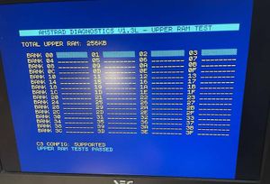
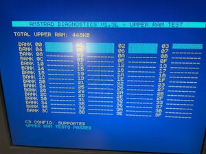
Now it's a good time to test if you have done everything right. Connect one of the A8 pins to GND with a wire and start the CPC. Run the diagnostics tool or a 128KB game. If you have done everything right, it should now behave exactly like a computer with 128KB built in.
Option A: TriPad stripboard
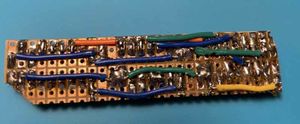
- Take a TriPad stripboard and cut out a part that is 2 stripes height has enough width to carry the 3 ICs plus capacitors.
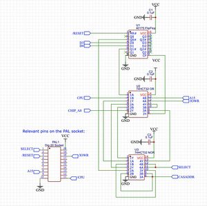
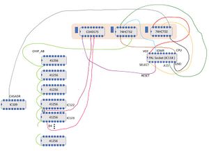
- solder the sockets to the stripboard according to the layout/schematics in the picture below
- solder the wires that go to other ICs on the mainboard to the stripboard
- now make all connections between the ICs according to the layout/schematics
- remove the PAL from its socket. Plug in another socket into the socket and solder all wires to their respective pins
- put the PAL into this socket
- finally connect the wires for chipA8, CASADR, D3 and D4 to the pins as documented in the diagram. (You can also use other soldering points as documented for the PCB below if they are more convenient.)
Option B: PCB
- solder the ICs and the capacitors to upper side the PCB
- if you want to disable the extension with a switch, also solder the resistor. The switch needs to be connected to the "disable" connection pads.
- if you have no intent to disable the extension, just bridge the "disable" connection pads with a wire. Don't populate the resistor.
- solder the PAL IC socket and the pin headers to backside of the PCB. The pin headers will later be pushed into the PAL socket on the motherboard. make sure they have quite the right length as if they are too long, there might not be enough headroom above the PCB for the keyboard and if they are too short, the connection might suffer.
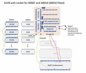
- connect chipA8 to one of the A8 pins of the new RAM chips and CASADR, D3 and D4 to appropriate connection points on the motherboard. The diagrams show some options. If you have mainboard with soldering points for the two different gate array versions, it's the most easiest way to use the soldering points there. Otherwise connections to IC pins are probably the easiest way.
- Remove the PAL chip from the socket on the motherboard (it's located right to the RAM banks, the 20pin IC in the socket) and insert it into the socket on the backside of the add-on PCB. Make sure you align its direction correctly . (Printed on PCB, Pin must face towards the pins of the IC next to it)
- Finally insert the PCB into the PAL socket on the motherboard. Make sure it's properly inserted.
important: double check wiring with actual Gate Array pinouts as I could not try all options
Construction of the 320/512K (PAL programming required) version
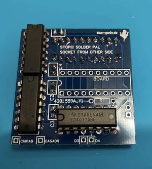
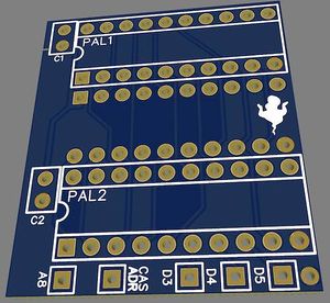
For a 512K version the biggest challenge is, that when we replace also the first bank we must treat the first 64K as base RAM and the other 192K as extended RAM in a way that it is properly recognised by software.
While this can be done with logic ICs it would need to much space to properly fit into a normal CPC6128. Instead this is achieved with two PAL ICs. ATF16V8 ICs are easy to find and relatively cheap but need to be programmed with e.g. an Eprom programmer like the widely available TL866-II.
What you need:
- The PCB - PCB Gerber files
- 2x Pin header 1x10
- 2x capacitor 100nF
- 2x ATF16V8 (or other PAL16L8 compatible ICs)
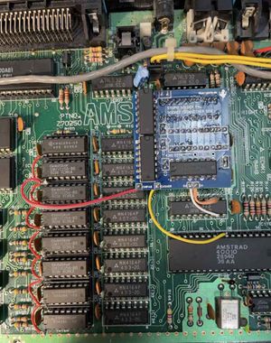
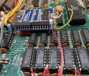
The assembly is pretty much identical to the PCB description above with the following changes:
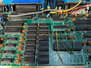
- replace both RAM banks with 41256 RAM ICs
- connect all A8 pins on both banks so that all 16 ICs are fully parallel on all address lines.
- program two ATF16V8 ICs with the attached JED files and solder them to the PCB
- There is a connection from the PCB to D5. D5 is e.g. pin 29 on the 40007 socket. For other options check the schematics/Pinouts.
Note: It's also possible to use this PCB as a 320K version. In that case only replace the second (left) RAM bank and connect the D5 pad to GND (throughhole directly next to the D5 pad).
References and links
- C't 512 KB internal RAM expansion
- Repair video on Youtube that shows how to remove RAM ICs and add sockets
- CPC Wiki forum thread
(eto)
