PAL16L8
Programmable Array Logic (PAL). Not to be confused with PAL, the colour encoding system for analog televisions.
The CPC6128 second page of 64KB RAM is controlled by a PAL chip.
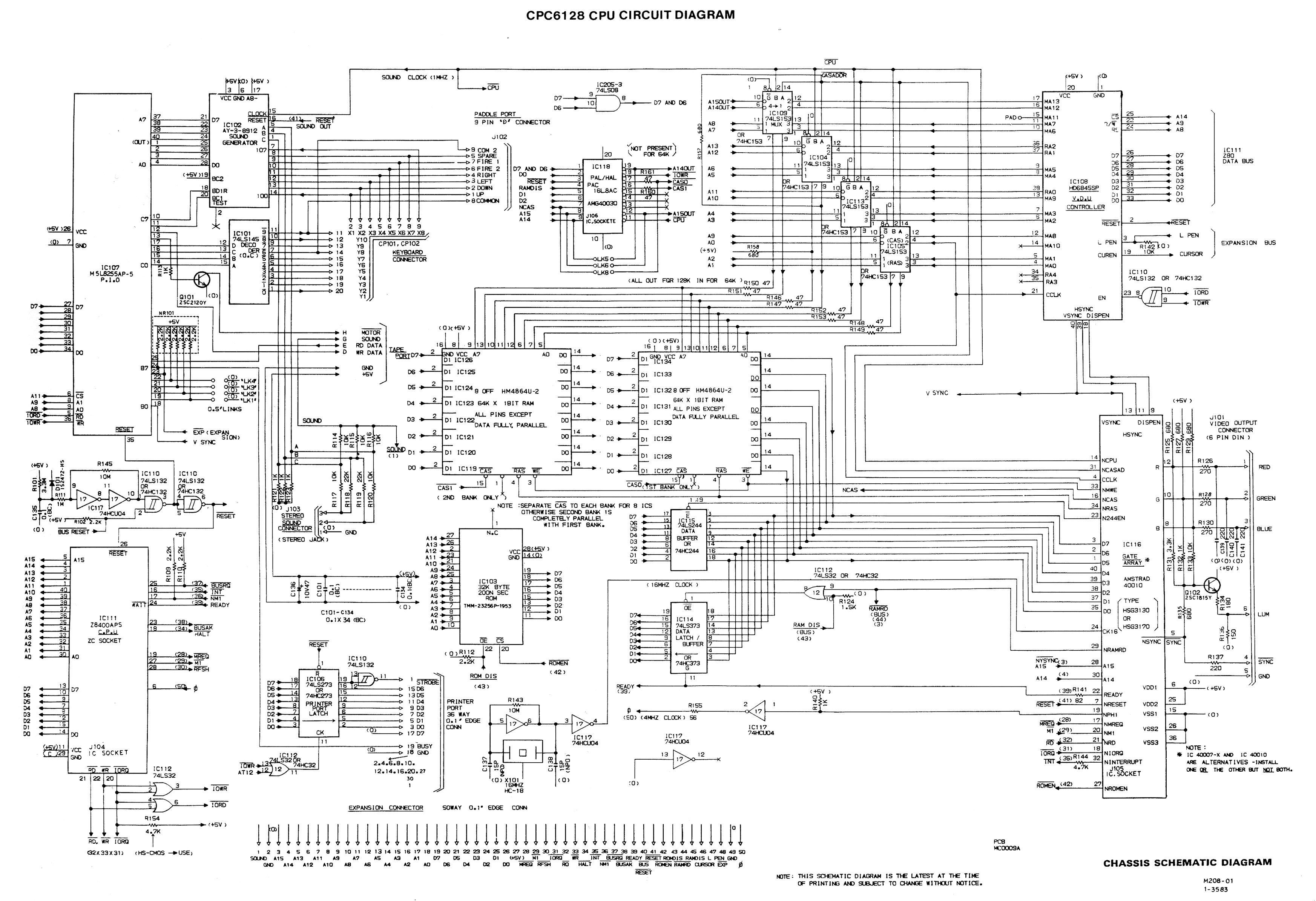
On the CPC 6128 schematic, it is top centre: CPC6128 Schematic however the X inputs aren't distinguished.
Contents
PAL I/O port
Note that no settings are stored in the Gate Array itself regarding the MMR register. But the PAL and Gate Array share an I/O port address so that it appears to be the same chip to the programmer.
Bit14 of the PAL selection address can be at 0 or 1 on CPCs equipped with CRTCs 3/4. It must be at 1 on CRTCs 0/1/2 (The result is not guaranteed).
For compatibility reasons, it is strongly advised to always set bit14 to 1 to select PAL. Furthermore, if bit14=0 then CRTC will be selected too.
The recommended I/O port address is &7Fxx.
Moreover, the PAL only respond to I/O Write requests while the Gate Array will respond no matter what the Read/Write I/O signal is. Source
PAL MMR register
This register controls how the extended RAM is banked into the CPU address space. It doesn't affect the video display at all (even in C3 mode). The Gate Array can only access the unmapped Base 64k page of RAM.
| MMR | 64K page | S | MM | CPU Memory Mapping | |||||||
|---|---|---|---|---|---|---|---|---|---|---|---|
| 7 | 6 | 5 | 4 | 3 | 2 | 1 | 0 | &0000-&3fff | &4000-&7fff | &8000-&bfff | &c000-&ffff |
| 1 | 1 | x | 0 | 0 | 0 | Base 64k / Bank 0 | Base 64k / Bank 1 | Base 64k / Bank 2 | Base 64k / Bank 3 | ||
| 1 | 1 | p | 0 | 0 | 1 | Base 64k / Bank 0 | Base 64k / Bank 1 | Base 64k / Bank 2 | Page p / Bank 3 | ||
| 1 | 1 | p | 0 | 1 | 0 | Page p / Bank 0 | Page p / Bank 1 | Page p / Bank 2 | Page p / Bank 3 | ||
| 1 | 1 | p | 0 | 1 | 1 | Base 64k / Bank 0 | Base 64k / Bank 3 | Base 64k / Bank 2 | Page p / Bank 3 | ||
| 1 | 1 | p | 1 | b | Base 64k / Bank 0 | Page p / Bank b | Base 64k / Bank 2 | Base 64k / Bank 3 | |||
On a standard 128k machine (unexpanded), bits5..3 are ignored. Page will always be fixed to Page 0.
Page order
RAM expansions are not required to conform to any page order. For example, the Dk'tronics Silicon Disc is a 256k RAM expansion that provides Pages 4 to 7.
RAM expansions can even be at an adjacent address range. For example, the Y-MEM is a 512k RAM expansion that uses the &7Exx range instead of the usual &7Fxx.
Given this diversity of RAM expansions, SymbOS does the right thing by testing each 64k page individually to detect the available RAM.
RAM mode &C3
The CPC 464/664 cannot deal with A14/A15 for Base 64k page like the 6128 does.
So external RAM expansions can differ in their behaviour regarding &C3 mode. See Discussion on the forum and Another discussion.
PAL Type Detection
10 OUT &7F00,&C0:POKE &4000,&C0
20 OUT &7F00,&C7:POKE &4000,&C7:OUT &7F00,&C0
30 IF PEEK(&4000)=&C7 THEN PRINT"PAL chip absent/inactive":END
40 OUT &3FFF,&C7
50 IF PEEK(&4000)=&C7 THEN PRINT"IO Bit14=0 PAL selected" ELSE PRINT"IO Bit14=0 PAL not selected"
60 OUT &7F00,&C0:POKE &C000,&C0
70 OUT &7F00,&C3:POKE &4000,&C3:OUT &7F00,&C0
80 IF PEEK(&C000)=&C3 THEN PRINT"Valid RAM mode &C3" ELSE PRINT"Invalid RAM mode &C3"
PAL and Pre-ASIC
The PAL component is integrated inside the Pre-ASIC chip. But it is disabled by default on the CPC 464.
It is possible to enable it by doing an hardware modification explained in that article: Arnold4
PAL and ASIC
The PAL component is integrated inside the ASIC chip. But it is disabled by default on the 464 Plus and GX4000. Source
Besides, most existing RAM expansions except Gemini have a problem. Source
The issue is specific to the Amstrad Plus machines which add yet another complication to the memory mapping handling on CPC machines. Basically, the ASIC can be memory mapped and hide a part of the RAM. This works well for the main RAM bank, and on the CPC, it also works for the internal extra 64K of RAM, which can be mapped at the same address. If you try to map both the RAM and the ASIC there, the ASIC is mapped and the RAM is not accessible until the ASIC is moved out of the way.
Unfortunately, memory expansions designed for the classic CPC does not take this into account. For some of them, because they were designed before the Amstrad Plus ASIC existed, and for some, the designers didn't think of it or decided it was not important. As a result, these extensions can enter in conflict with the ASIC, which will result, at best, in software crashes, and at worst, in damage to the hardware.
Software that is known to hit this problem with existing memory expansions:
Signals used for RAM management
The following signals are used for RAM management and are available on the expansion connector.
RAMDIS
(Internal RAM Disable; Input to Internal RAM)
When RAMDIS="1" the internal RAM of the CPC/CPC+/KC Compact is forced inactive. e.g. a ram-expansion device would use this signal to override the internal RAM selection with the RAM on the device. The internal RAM would be forced inactive, and the RAM on the ram-expansion would be actived.
/RAMRD
(RAM Read; Output from Gate-Array)
When /RAMRD="0" a ram read operation is active. This signal is generated by the Gate-Array. This signal will be "0" when:
- A15=A14="0" and bit 2 of the Gate-Array rom configuration register is set to 1. (lower ROM disable)
- A15=A14="1" and bit 3 of the Gate-Array rom configuration register is set to 1. (upper ROM disable)
- A15 is not equal to A14.
Initial replacement equation (Porchy)
The following equations were worked out by Porchy (member on CPCWiki Forum) to program replacements:
A15OUT = (!X2 & !X1 & A14
     # !X3 & !X2 & A14
     # A15);

!X1 = (!A15 & D7ANDD6 & RESET & !IOWR & D0
     # !X1 & RESET & IOWR
     # !X1 & !D7ANDD6 & RESET
     # !X1 & A15 & RESET);

!X2 = (!A15 & D7ANDD6 & RESET & !IOWR & D1
     # !X2 & RESET & IOWR
     # !X2 & !D7ANDD6 & RESET
     # !X2 & A15 & RESET);

!X3 = (!A15 & D7ANDD6 & RESET & !IOWR & D2
     # !X3 & RESET & IOWR
     # !X3 & !D7ANDD6 & RESET
     # !X3 & A15 & RESET);

!CAS1 = (X3 & !X1 & A15 & A14 & !NCAS & !RAMDIS & !CPU & CAS0
     # !X3 & !A15 & A14 & !NCAS & !RAMDIS & !CPU & CAS0
     # X3 & !X2 & X1 & !NCAS & !RAMDIS & !CPU & CAS0
     # !NCAS & CAS0 & !CAS1);

!CAS0 = (X3 & X2 & X1 & !NCAS & !RAMDIS & CAS1
     # X3 & !X1 & !A15 & !NCAS & !RAMDIS & CAS1
     # !X3 & A15 & !NCAS & !RAMDIS & CAS1
     # !X1 & !A14 & !NCAS & !RAMDIS & CAS1
     # !X3 & !A14 & !NCAS & !RAMDIS & CAS1
     # !NCAS & !RAMDIS & CPU & CAS1
     # !NCAS & !CAS0 & CAS1);

A14OUT = (A15 & A14
     # !X1 & A14
     # X3 & A14);
File:Amstrad6128.jed Original JED File posted on CPCWiki Forum
Fixed version (Gerald)
Original version from Porchy suffers from a bad handling of the RAMDIS signal. It caused screen artefact when accessing an external RAM expansion.
A14OUT     = !(  !A14
             #   !A15 & !Q0 & Q2 );

A15OUT     = !(  !A15 & !A14
             #   !A15 & !Q1
             #   !A15 & !Q0 & !Q2 );

Q0     = (  D7ANDD6 & nRESET & D0 & !A15 & !nIOWR
         #   !D7ANDD6 & nRESET & Q0
         #   nRESET & A15 & Q0
         #   nRESET & nIOWR & Q0 );

Q1     = (  D7ANDD6 & nRESET & D1 & !A15 & !nIOWR
         #   !D7ANDD6 & nRESET & Q1
         #   nRESET & A15 & Q1
         #   nRESET & nIOWR & Q1 );

Q2     = (  D7ANDD6 & nRESET & D2 & !A15 & !nIOWR
         #   !D7ANDD6 & nRESET & Q2
         #   nRESET & A15 & Q2
         #   nRESET & nIOWR & Q2 );

nCAS0     = (  nCAS
            #   RAMDIS & !nCPU & nCAS0
            #   !A15 & A14 & !nCPU & Q2 & nCAS0
            #   A15 & A14 & !nCPU & Q0 & !Q2 & nCAS0
            #   !nCPU & !Q0 & Q1 & !Q2 & nCAS0
            #   !nCAS1 );

nCAS1     = !(  !RAMDIS & !nCAS & !A15 & A14 & !nCPU & Q2 & nCAS0
            #   !RAMDIS & !nCAS & A15 & A14 & !nCPU & Q0 & !Q2 & nCAS0
            #   !RAMDIS & !nCAS & !nCPU & !Q0 & Q1 & !Q2 & nCAS0
            #   !nCAS & !A15 & A14 & Q2 & nCAS0 & !nCAS1
            #   !nCAS & A15 & A14 & Q0 & !Q2 & nCAS0 & !nCAS1
            #   !nCAS & !Q0 & Q1 & !Q2 & nCAS0 & !nCAS1 );
File:CPC6128.JED : Fixed version of Amstrad 40031 GAL replacement
File:CPC6128.hex : Fixed version of Amstrad 40031 GAL replacement, Hex Intel version.
Internal PAL on CPC 6128

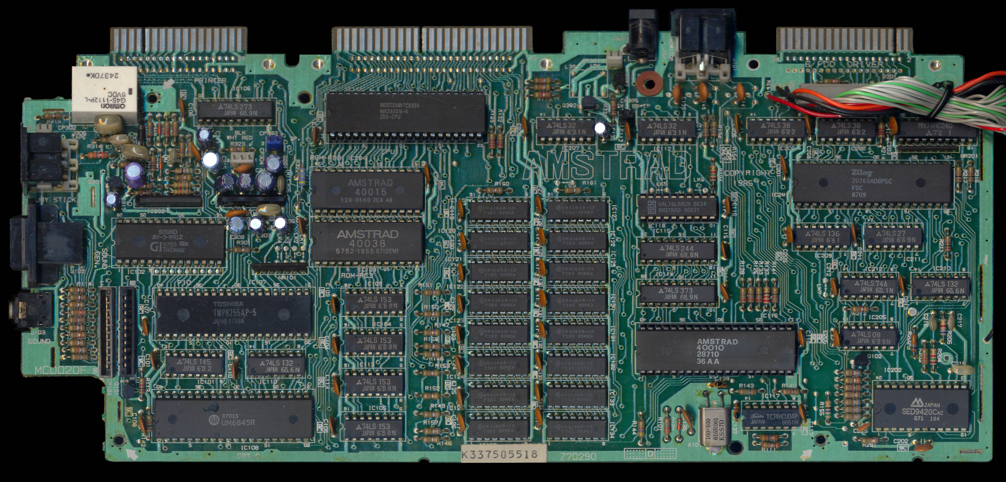
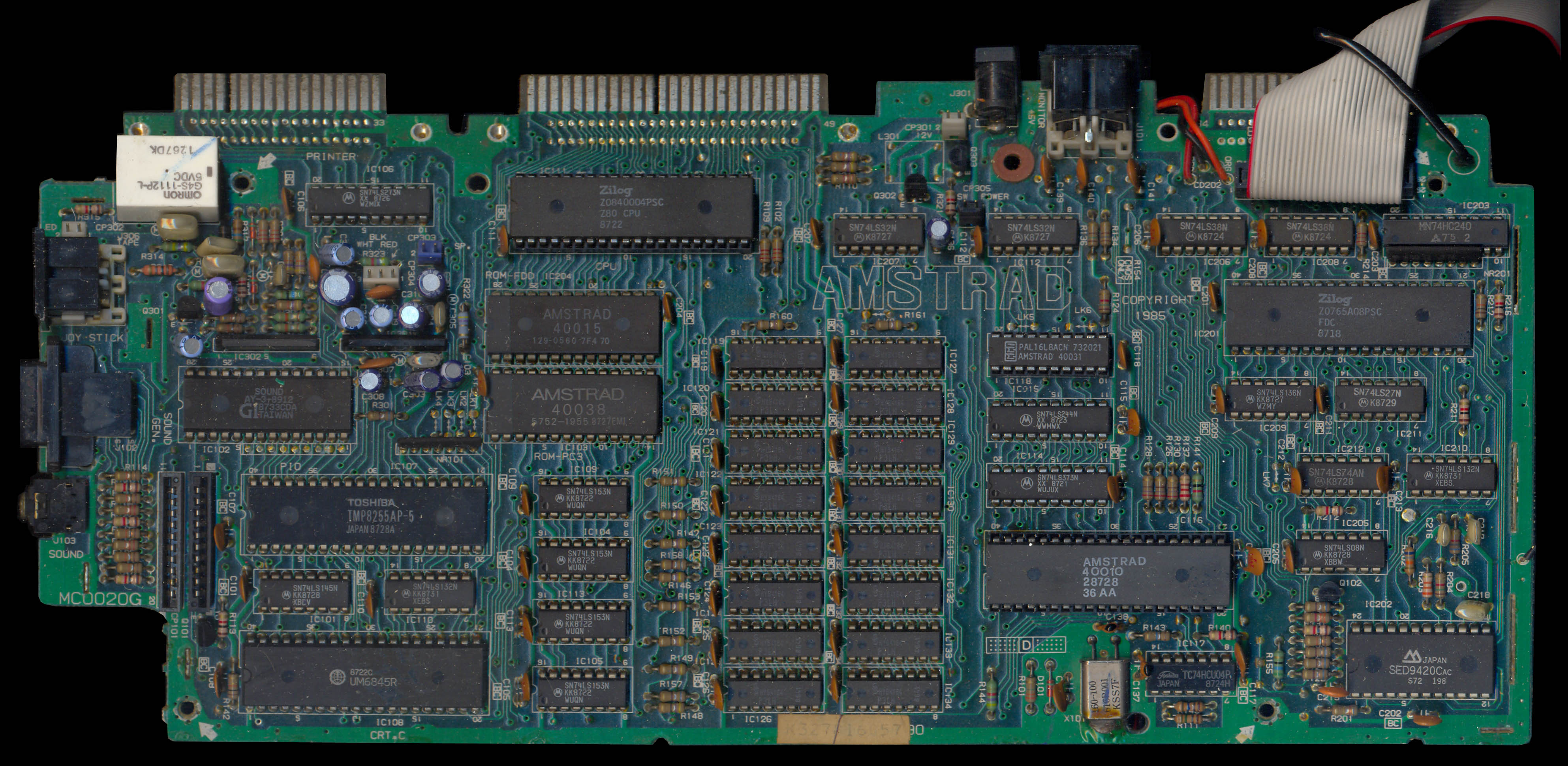
IC Models used in CPC
These are the ones known to be used in the CPC by looking at pictures of CPC mainboards:
They both wear the same Amstrad part number 40031. On the Amstrad chassis schematic diagram, this part is numbered 40030. Source
576KB vs 640KB total
Bits 3, 4, 5 allow to define up to 8 pages of 64K for RAM expansion at a given address range in addition to the 64K base RAM. The internal second 64K RAM bank of the CPC 6128 is usually disabled when a RAM expansion is used, as the 64K enhanced RAM in the 6128 would use the same address range (&7Fxx) as the first 64K of the RAM expansion. This gives you 576K of total RAM on a CPC.
However, if the RAM expansion decodes the A8 address line, you can access the internal second RAM bank of the 6128 from another range (&7Exx). The X-MEM and iRAM/640 expansions implement this and therefore can provide 640K of total RAM. Source
4MB RAM expansions
Beware about 4MB RAM expansions. The upper 2MB (Port 7Bxxh, 7Axxh, 79xxh, 78xxh) of a 4MB RAM expansion can conflict with other hardware as setting A10 to 0 is also used for many hardware expansions.
See the I/O Port Allocation Rules to understand why.
The practical safe maximum on Amstrad CPC with Standard Memory Expansions is 2MB.