FPGAmstrad
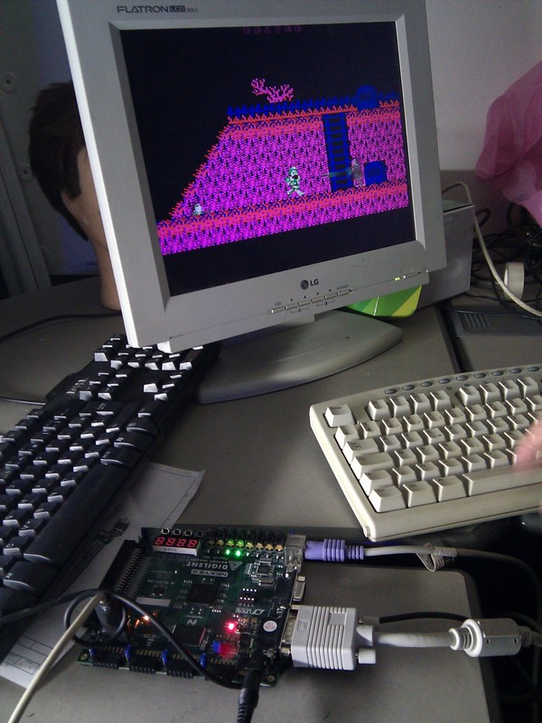
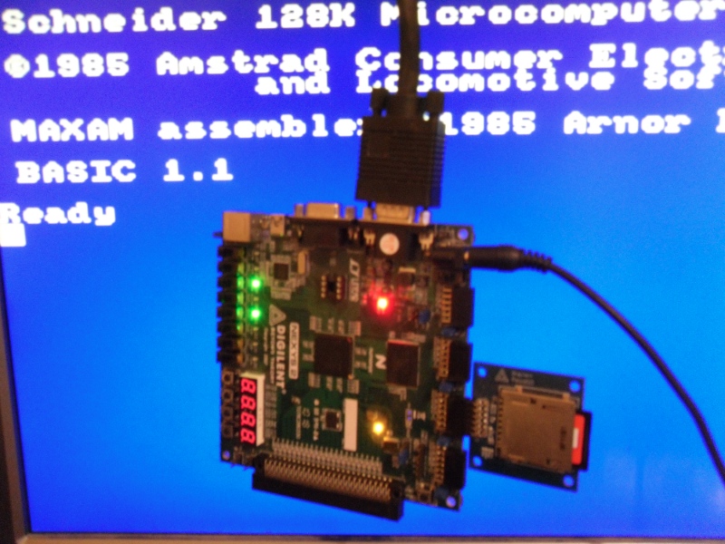
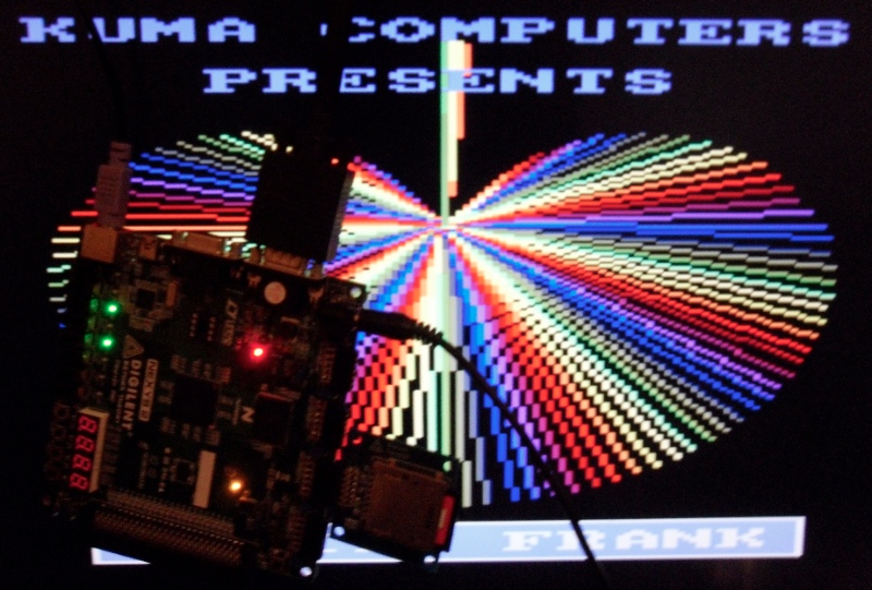
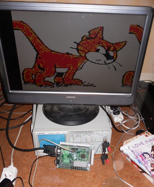
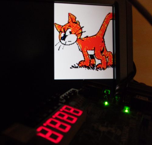
This is a VHDL version of Amstrad CPC 6128 running on FPGA starter-kit NEXYS2 500k-gates from Digilent. A starter-kit is a board made for learning FPGA, so it is a standard FPGA development board.
Please refer to [MiST-board CoreDocAmstrad] for the final user version, running on MiST-board platform.
Some games running on it : 1942 1943, 3D grand prix, A view to a kill, Action Fighter, animated strip poker, Antiriad, Arachnaphobia, Arkanoid, Arkanoid Revenge of Doh, Asphalt, Axiens, Barbarian MH, Barbarian PA, Barbarian II, Battleships, Bomb Jack I and II, Boulder Dash, Bruce Lee, Bubble Ghost, Buggy Boy, Bully's Sporting Darts, Cauldron I and II, Chase HQ, Chicken Chase, Classic Axiens, Classic Invaders, Crazy Cars, Crazy Snake, Dan Dare I II and III, Dizzy 7, Donkey Kong, Double Dragon I and II, Druid, E-Motion, Exolon, Express, Fruity Frank, Ghost'n'Goblins, Golden Axe, Gryzor, Heart Land, Hold-up, Hyper bowl, Ikari Warriors, Impossible Mission, Invasion of the Zombie Monsters, Iron Lord, Killapede, Klax64, Laser Squad, Light Force, Locomotion, Lode Runner, Macadam Bumper, Mange-Cailloux, Mario Bros, Maze Mania, P47, POP-UP, Prince of Persia, Prohibition, Realm, Rebel Star, Rick Dangerous I and II, R-Typeee, Rock Raid, Rogue, Rygar, Salamander, Sapiens, Shinobi, Sim City, Sorcery, Spectra, Spherica, Spin Dizzy, Star Ranger, Star Quake, Star Wars, Strider II, Super Ski, Superkid In Space, Tank Command, Tempest, Tetris 95, The Duct, The Empire Strikes Back, Trail Blazer, Trakers, Turbo Tortoise, Turrican I and II, Venoms, Victory Road, Vixen, WEC Le Mans, West Bank, Wizard's Lair, Word Cup Challenge, Word Series Baseball, Xevious, Xor, Zolyx.
Contents
- 1 How to assemble it
- 2 Video
- 3 Last news about this project
- 4 Contact
- 5 Tests done
- 6 Effort done
- 6.1 Instruction timing
- 6.2 Test of a real Zilog 80
- 6.3 Alignment of HSYNC Interrupt
- 6.4 ram_palette
- 6.5 Sniffing of a real Amstrad
- 6.6 ROM and RAM extension
- 6.7 Sound output
- 6.8 DONE: Another disk selector
- 6.9 TODO : A X/Y input
- 6.10 DONE: A SCART output
- 6.11 DONE : CRTC1
- 6.12 TODO : Interlaced scanlines
- 6.13 DONE : Scanlines
- 6.14 DONE : Monochrome option
- 6.15 TODO : Ethernet
- 6.16 TODO : arnoldemu's testbench fdctest
- 6.17 TODO : github migration
- 6.18 PPI
- 6.19 TODO : a better border heuristic
- 7 Agile method
- 8 Platforms
- 9 MiST-board - Core Developer's Notes
- 10 Source code
- 11 Schematics
- 12 Components
- 13 And thanks
How to assemble it
You need:
- a "NEXYS2 500kgates" starter kit from Diligent [[1]] (1200kgates should be better for future version => in fact I choosen NEXYS4, it is same RAM inside) also in France : [[2]] or in Germany : [[3]]
- a "PMODSD" module for reading sdcard [[4]]
- an alimentation (cause they don't give it with starter kit) [[5]]
- optionally a DIGILENT USB JTAG (normally starter kit can be programmed directly by usb, but I don't have tested this way) [[6]]
- a 4GB SDCARD (no more), I have exactly a "SDHC 4GB class4 Verbatim"
- the binary of this project (candidate 002) : source+500k-gates binary [[7]] ; 1200k-gates binary [[8]]
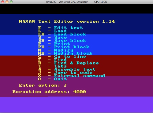
- several ROM files: OS6128.ROM BASIC1-1.ROM AMSDOS.ROM (from JavaCPC[[9]]); MAXAM.ROM[[10]]
- one or more DSK files : TEMPEST.DSK[[11]] ARKANOID.DSK[[12]] FRUITY.DSK[[13]] BRUCELEE.DSK[[14]] CHASEHQ.DSK[[15]] WIZLAIR.DSK[[16]] XEVIOUS.DSK[[17]] BOULDER.DSK[[18]] CLASSIC_AXIENS.DSK[[19]] CLASSIC_INVADERS.DSK[[20]] GRYZOR.DSK[[21]] PRINCE.DSK[[22]] BUGGY.DSK[[23]] TRAIL.DSK[[24]] P47.DSK[[25]] SUPER_SKI.DSK[[26]] ACTION_FIGHTER.DSK[[27]]
A package that contains minimum set of ROM and DSK for filling simply sdcard [[28]] (OS6128, BASIC1-1, AMSDOS, MAXAM)
You have to:
- program FPGA with the binary file "amstrad_switch_z80_vga_sd.bit" of this project, for it I use Digilent Adept software and my USB JTAG cable
- format your 4GB SDCARD in FAT32 4096 byte allocation size
- copy ROM and DSK on SDCARD
- plug PMODSD on slot JC1 of starter kit, and set all 8 switches to 0
- plug VGA, and turn on starter kit
You can:
- plug a PS/2 keyboard, and type "cat"
- increment switch to select another disk at boot, if screen became RED, it's that binary value done by switches is too big, leds are doing a small animation when a disk is correctly loaded
- plug principal joystick on slot JB1 (Vcc 3.3v is common)
- plug another joystick on slot JA1 (Vcc 3.3v is common)
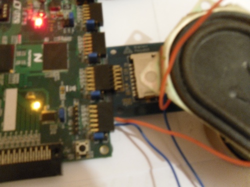
- plug a jack on slot JD1, one at upper GND plug, and second wire at next plug, just at left of it (if it was 3.3v Vcc, choose the right one instead)
Wires are plugs at upper part of pmod D.
From bottom to upper: [nothing: Vcc 3.3v] [blue: GND] [red: sound]
Sure you can connect a jack...
And two joysticks. On pmod B: bottom is (both) 3.3v, so joystick's common, next is (both) GND (not used), and others are joystick connections, to test manually :)
Video
http://www.youtube.com/watch?v=Z8FB_eIy8LY
Last news about this project
In September 2016, FPGAmstrad does use external RAM as RAM+VRAM, no more "LowerVRAM/UpperVRAM" switches to select in OSD menu.
In August 2016, FPGAmstrad does pass some arnoldemu's testbench : PPI PSG CPCTEST.
In February 2016, FPGAmstrad has a TV mode (original signal)
In September 2016, FPGAmstrad has write access on both disk drives, and can change dsk.
In March 2015, FPGAmstrad is stable on MiST-board, please refer to MiST-board CoreDocAmstrad and mist-board amstrad bin core
In December 2014, FPGAmstrad is stable on NEXYS4, WIP, BOOTLOADER improved, VRAM improved (with BORDER colors !), RAM relaxed, no more timeout in keyboard key-press, Ghouls 'n' Ghosts, Macadam, a lot more to do. 14% of platform is used.
In November 2014, I bought MiST board, with two pro joysticks.
In September 2014, I bought NEXYS4, more powerfull than NEXYS2, with same external RAM, internal mini-sd, no PS/2 (it is a pmod option)... I have some patchs to make (MSB FAT32 offset). I would like to make a USB snifer also with it (usb to ethernet (wireshark))
Contact
I am Freemac, my IRL name is Renaud Hélias.
You can contact me by mail to renaudhelias @t gmail d0t com, if you have questions about assembling this project.
Follow me on my google plus account!
Tests done
Great games that are running properly are listed at top of page.
On MiST-board CoreAmstrad version
Games that doesn't run are :
- ACPC_logon_system.dsk: text scrolling lag. This demo will be used for horizontal ink calibration (when I’ll buy a luxurious FPGA platform... I need in fact 224KB of internal RAM to do it), and CRTC overcounts.
- commando.dsk: pixels that should be deleted are not deleted (only VRAM &C000-FFFF seems used)
- split ink demo.dsk: (from cpcrulez) : may help about ink raster calibration.
- Sultan's Maze.dsk: does need the right part of keyboard (F0-F9 are used for directions in this game)
- Orion Primes.dsk: does display "secteurs entrelacés" - "vérifiez votre copie", a FDC problem.
- Batman_Forever.dsk: some problem during flying chip demo part, and several rupture showing ghost lines around Vcc=0.
- 30YMD.dsk: in Benediction demo, at bottom some time you see some ghosts of central animation (too many HSync per screen ?)
- arkanoid2.dsk: don't run in r005.8.13, but fine in r005.8.13e (experimental fork)
- trailblazer.dsk: no more "raster" problem since r005.5, it's now perfect ! Palette heuristic offset (done for unlocking Batman Forever Demo) has a small effect in left (squares are not separated by a black line in first column)
- imperial_mahjong.dsk: modern EXA/EXA2 resolution not passing my color pallet heuristic :p
- rtypeee.dsk: at begin of presentation, a draw of "jack plug" is done in a strange video mode, more than 200 pixels of height !, see flipping lace
- S&Koh.dsk: LOGON SYSTEM, black screen in r005.8.4... damn
- Pinball_Dreams__PREVIEW.DSK: Does run in experimental/ versions r005.8.9.2 and r005.9.11e (experimental forked version of r005.9.11 using flag FPGAmstrad_amstrad_motherboard.vhdl.HACK_Z80=false). Does freeze in !experimental versions when background music is special (not long classic background music) and you press two buttons (left/right flipper keys) at the same time.
Arkanoid.dsk stars use rupture address (changing address several time during display of one image), it is now supported on "candidate 001" version of FPGAmstrad. Run better in r005.9.11e than in r005.9.11.
Gryzor and Prince of Percia use rupture ink/mode (changing ink and mode during display of one image), it is now supported on "candidate 002" version of FPGAmstrad
Gryzor is really sensitive to Amstrad general stability : do press esc at start menu does activate music during game, if no music, FPGAmstrad is in an instable version (last known stable version r003.8)
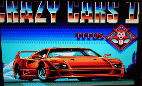
Crazycars2.dsk first car image use 32KB of VRAM, it is now supported on "candidate 001" version of FPGAmstrad.
Ghouls'n'Ghost.dsk / Ecole.dsk does need RAM write when writing in ROM (RAM is beside ROM, hard to emulate with asynchronous SDRAM controler, MiST does use a hacked synchronous RAM done for that)
moktar.dsk / super_cauldron.dsk does run fine since r004.8.1.1.
CPC Aventure does run fine since r005.2 (message about turning disk now displayed)
prehistorik.dsk does run fine since r005.2 (key can now be pressed in intro demo)
Sim City and Hero Quest run fine since r005.2 (it was about "key always pressed"), but does need a hard boot (not quick reset keyboard key), certainly a small problem of component init state.
A lot of demos don't pass in NEXYS4 FPGAmstrad's version (I need to implement back the SDRAM hacked in MiST board FPGAmstrad version). CPCRULES demos is a cool ressource as it contains simple dsk formats.
crazycar.dsk does use lowerVRAM=00 (&0000-3FFF and &C000-FFFF area for VRAM)
crazycar2.dsk does use lowerVRAM=10 (&8000-BFFF and &C000-FFFF area for VRAM) while overscan presentation, and lowerVRAM=00 (&0000-3FFF and &C000-FFFF area for VRAM) during play. Run fine since r005.7
buggyboy.dsk: I found one dsk running correctly and another not : problem on this last one is about turning left/right effect : the car continues straight (it seems a prototype bad version)
superski.dsk : don't forget to disable autofire, in jump, do press fire+up or down.
protext.rom: All right since r004 (before, in edit mode, if I pressed continuously one key, it did write ten letter and freeze/crash. Do note that a number is incremented in live at top right, so this is a complex software, good for keyboard vector stability tests)
atomdriv.dsk: unlocked since r004.5 (the game and music did freeze (ROM unplugged shall return xFF))
rtypeee.dsk: unlocked since r004.7. Does use special read FDC cmd, with BOT different of EOT (begin of track/end of track), so reading several 512 bytes blocks in one FDC command only.
Arkanoid Revenge of Doh and Asphalt are two games that doesn't support ROM extensions : Doh starts to show small bad layers, and Asphalt does crash and reset before main menu... if you add another gadget ROM.
antiriad.dsk: no keyboard/joystick between r004.5 and r004.7. By adding pull-up at r004.5 I lost this game, by implementing a better PPI in r004.8 this game run fine : Antiriad is back !
-circles.dsk: this demo freeze does since r004.8 (PPI border effect ?) and is back since r005.5, it was nice to calibrate SOUND clock : I did generate 8 candidates of synchronizing this clock (1MHz from 4MHz : 1100 0110 0011 1001, and 0.5 deltas : 1100i, 0110i, 0011i, 1001i), only one does not freeze -circles... so I release r005.5 candidate. This demo is a great one around calibrating Yamaha clock.
Nigel Mansell's Grand Prix.dsk: Only one race track seems ok : Monaco (Brazil track does not start). Unclassified : this disk bug also with other emulators, certainly a bad dsk dump here, TOSEC version of Nigel Mansell does run fine (but some legendary traces of "SK bit purpose" needed by here (in FDC, setting SK does jump deleted disk tracks), perhaps to investigate)
saboteur2.dsk: run fine since r005.5 (nice music and then freeze problem), it was about Yamaha clock generator (generated by Gatearray, versus WAIT_n added in short Z80 instruction to let them during all 4 clocks (Z80 in Amstrad does use 4T or 8T instructions (WAIT_n does insert missing T)). Does freeze at welcome since r005.8.7. Back since r005.8.10.
tetris95.dsk : bad in r005.8.9.2 (4 beep while breaking 3 lines (instead of 3 beep while breaking 3 lines), was correct in r005.8.4. Back since r005.8.10.
| Game | Welcome | Title | Game |
|---|---|---|---|
| CrazyCar2 | 1011 | 0011 | |
| One | 0111 | 0011 | |
| Scarabus | 0111 | 0011 | |
| Ace | 0010 | ||
| Tintin | 0111 | 1011 | 0111 |
| Devil's Crown | 0001 | 0011 | |
| Mach 3 | 0111 | 0111 | 0110 |
| Paranoia (1994) | 1011 | 0001 | |
| World Class Rugby | 1011 | 0001 | 0001 |
| Miam Cobra | 1001 | ||
| Galivan | 0001 |
XOR.dsk does use lowerVRAM=01 (&4000-7FFF and &C000-FFFF area for VRAM)
TODO :
- To test also : Unlimited Bobs (Dr.Piotr).dsk demo.
Effort done
Instruction timing
I tested instruction timing of T80 compare to instruction timing of JavaCPC emulator. I deduce synchronization of Z80 with CRTC on M1 signal by WAIT_n insertion in order to have a multiple of 4 Tstates per instruction. I deduce also one WAIT_n inserted during MEM_WR operation (yes I log testbench T80, I’m crazy)
I just made a test bench log of T80 (log of instruction's M1, and first M1 coming after knowing that I send a lot of NOP after my instruction), and compare it to a JavaCPC timing array. Some instructions was not tested (interrupt wait, and special timing (instructions with change timing)), but all others passed correctly.
Instruction timing : currently in r008.5.14
In GA, I do use begin of edge for IO_ACK instead of state.
M1 reached same time of IO_ACK are ignored (not M1) in WAIT_n generator.
MEM_WR has an OSD menu choice to switch between "quick" and "slow", "slow" mode does insert ONE WAIT_n during detection of MEM_WR. This switch exists because somes games are running in "slow" mode and others in "quick" mode.
Instruction timing : talk about r008.5.14
In fact it exists several instruction making MEM_wr, and adding each one ONE WAIT_n does result in different case of synchronization.
If it's about managing GA reading pixels, perhaps not only M1 signal are synchronized but also the MEM_RD and MEM_WR accesses at another offset.
Timings instructions Z80 sur CPC
If interruption r52 is regular, even while making a continues MEM_WR, interruption (int<='1') shall be taken into account above WAIT_n insertions ?
In Z80 sequence diagram, an IO_ACK(+M1) is preceded by M1 (single)
cpctest.dsk -Timing Instruction- is different while using mode "MEM_WR=slow" and "MEM_WR=quick". Strangly better using "MEM_WR=quick".
Current version is using "Z80_HACK=true" (parameter set during compilation), that shunt Z80.WAIT_n entry, Z80.clock is slow down during theses WAIT_n. It's the only current way I succeed in slowing down enough Timing Instruction for unlocking Saboteur 2 game.
Key games here are : Saboteur 2 (run fine with "MEM_WR=slow", does freeze with "MEM_WR=quick") and Arkanoid II (run fine with "MEM_WR=quick", too slow using "MEM_WR=slow")
CPC Z80 Commands and how long they take...
Test of a real Zilog 80
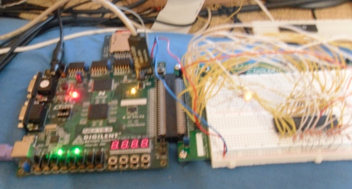 Code name : Z80fx2bb, real Z80@2MHz (instead of 4MHz) on fx2bb extension card.
For it I plug all wires simply from 1 to 40. Some wires are cut, some are Vcc, others GND. Z80 output are directly connected, Z80 input are pull-up with red-red-red resistors (I like red), Z80 is powered 5v (pmod can give 5v using jumper). In fact z80 is so old component that powering it 5v do output 3.3v.
In fact the only difference between T80 of opencore and real Z80 is that T80 run on rising_edge, and Z80 run during low state. Test past with little modification of sequencer forcing it do nothing during low state of z80, resulting a downclock (memory is too overclocked with this sequencer modification), perhaps using buffer on address bus and data bus could solve this detail... but as it runs for me it is not a problem.
TODO : Z80 testbench
CPC-Power Z80 FULL TEST (UK) (2012) - UTILITAIRE
Some errors detected in r005.8.4 (test done by Philippe D.)
WinAPE plustest.zip (including Instruction and Interrupt timing tests)
Alignment of HSYNC Interrupt
Interrupt are respected since version "candidate 001" of FPGAmstrad.
JavaCPC running norecess's "using-interrupts" code [[29]]
It could be interesting to test this asm code on next version of FPGAmstrad.
TODO : arnoldemu testbench - cpctest
forum : amstrad cpc "acid" test => I have uploaded updated tests : http://cpctech.cpc-live.com/test.zip
Tests done here : ppi/psg/cpctest.
In r005.6, I reach successfully some arnoldemu tests to calibrate more efficiently HSYNC interrupt : ppi.bin, psg.bin, cpctest.bin.
Games unlocked by r005.6 : Sigma7, Pac-land, Golden Tail.
In r005.8, Prehistorik is running fine.
In r005.8.4, arnoldemu testbench "cpctest" does fail :/
In r005.8.7, arnoldemu testbench "cpctest" is OK
In r005.8.14 version, using default mode "MEM_wr:quick", is OK. And Prehistorik II is running fine.
TODO : arnoldemu testbench - crtctest
Adding choice of CRTC 0 or 1 on OSD, and passing this test could be great.
ram_palette
VRAM contains 800x300 amstrad pixels (VZoom x2), displayed VGA 800x600@72Hz with fix regular border at 768×576 and fix inside border at 768×544.
- simple_GateArrayInterrupt.vhd (GA to VRAM) parameters : VRAM_Hoffset/VRAM_Voffset
- aZRaEL_vram2vgaAmstradMiaow.vhd (VRAM to VGA) parameters : H_BEGIN/H_END/V_BEGIN/V_END (theorical fixed values)
To calibrate : VRAM_Hoffset++ does offset one char left. VRAM_Voffset++ does offset one line up. On display H_BEGIN does begin to scan lines of VRAM. But V_BEGIN does not enter in consideration here : vertical=0 does begin to scan columns of VRAM.
In original CPC, top border has 1/2 char more than bottom border. I used Batman Forever default welcome/calibration screen to calibrate VRAM offsets.
RAM_palette contains the ink list and the mode for each line of VRAM, sampled at horizontal middle of 800x600 screen, and used at begin of each line.
Sniffing of a real Amstrad
I listen to some wires of my Amstrad CPC 6128 plus, but I can't access VSYNC/HSYNC output of CRTC, so I have to buy another model in order to do this test. In fact you can listen at clock of Amstrad and transmit it to FPGA DCM component, resulting a accelerated clock sequence, that's it, with FPGA DCM you can overclock output Amstrad clock signal in order to insert more operations, I use this tip for listening signals and save them inside starter kit asynchronous RAM (write, stop write, write, stop write... I’m a perfectionist paranoid...)
You can power Amstrad CPC using extension port, applying 5v. By doing it, power down button of Amstrad doesn’t run. Using this way you reach a common 5v power between starter-kit and Amstrad. I connected wires from extension port directly to FPGA, as they are used just for listening.
ROM and RAM extension
In r004, you have more RAM +512KB, and you can add ROMs.
- LowerROM has .eZZ file extension
- UpperROM has .e00 ot eFF file extension (hexa)
In r005.4, I add another UpperROM set : .f00 to .fFF file extension (hexa). If you press "space" during a reset_key ("page up" key), upperROM files used range from .f00 to .fFF instead of ranging from .e00 to .eFF. LowerROM .eZZ file extension is still used in both case.
Sound output
PWM
Using a simple PWM, data is entered at a certain speed, the PWM clock speed.
If you simulate a constant PWM output signal at middle range of voltage (state just between 0V and 5V : 2.5V), it results an alternance of 0V and 5V, that result in a noise sound. In Arkanoid, this defect make some continues sounds instead of silents...
My idea is generating a sound having a frequency upper than dog ultra sound, while I want to simulate a constant 2.5V.
For this I do use two clocks entries in my PWM : one about data entry, and another about algorithm execution.
This result a high quality sound output (in addition to this nice Yamaha sound chip from fpgaarcade)
Stereo sound output
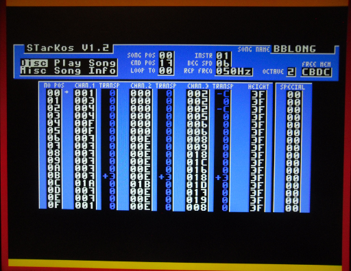
Sound chip was modified in order to get channel A+B at left, and channel B+C at right. It was tested OK using STarKos 1.21 sound tracker (track "Carpet")
DONE: Another disk selector
In first version of FPGAmstrad (NEXYS2) I used switches for disk selection. As final FPGA platform doesn't have any switches set, I have to add an BASIC instruction for it, something like "OUT &CAFE,disk_number" could be fine.
Since FPGAmstrad in NEXYS4, disk selection is done from keyboard, using "OUT &CAFE,disk_number" instruction. A reset key was added also. "PRINT INP(&CAFE)" does print current disk selected number.
DONE : A advanced dsk drive
Done on r004, I added also a second Drive in order to copy easily files from one disk to another.
Irregular sector size ok.
You just have to select Drive A or B from OSD before selecting another dsk file.
Write is done directly on sdcard dsk file, so you can save games, and write texts...
You can now change disk without reset. And then play games using several disks.
CPCWiki forum - Amstrad CPC hardware - FDC floppy t80ds detection : talk about FDC in MiST-board CoreAmstrad.
DONE : A advanced FDC (with write access and more)
Since r004 "mecashark", the FDC implementation has write access !
UNDONE : FAT32 fragmented files support
Since advanced FDC, dsk files have to be defragmented. Only ROMs are safe with a not defragemented sdcard...
TODO : SNAP DSK
Add an option in OSD MENU : "SNAP DSK". Does create a copy of current disk in current drive into "SNAP[number].DSK". Heuristic for number : file count (at boot, incremented at each snap dsk done)
TODO : fix message "This program will not run in this environment. Press any key"
HartOz
The core does not support the bundled CP/M+ software.
With a valid working CP/M+ Disc1 image mounted, the systems returns with the following message after issuing the |cpm command.
"This program will not run in this environment. Press any key"
"Wrong disk for your configuration" message seen in one-disk version of "Batman Forever" demo (two separate disk version runs fine)
Do fix also message "Bad Command" while running a not existing file on disk.
Certainly linked to Orion Primes.dsk loading problem.
TODO : A X/Y input
I want to work also on screen-pen entry, is there a manner to detect an analog X/Y as pen or gun ? YES : Markus Hohmann does it, he implements the lightgun on JavaCPC-GX4000 using mouse :)
http://cpcrulez.fr/hardware-pistolet-magnum_light_phaser_ACPC.htm
register 11,12 and 13 ?
DONE: A SCART output
In order to plug FPGAmstrad on TV, and help debugging. And also to test a simple scan-doubler.
r005c17 : experimental version, original signal TV output is running fine, with OSD menu. Have to add a flag in mist.ini instead of using OSD menu. scan-doubler doesn't run ok in mode 2, and has strange offset with Arkanoid (vertical display games), so it unvalidated : only original TV output will be added to r004 in r005.
r005 : VGA 60H/TV 50Hz.
TODO : A SCART output with border
Original output signal has no border, I have to implement the original border in TV mode.
Priority: HIGH! (asked by Markus Hohmann)
DONE : move SCART parameter into mist.ini
Doing like in other cores : do use the global "scandoubler" option in mist.ini to switch between VGA and TV mode.
TODO : mix SCART H and V sync into HV sync (sort of C sync)
Amstrad CPC core · Issue #35 · mist-devel-mist-binaries · GitHub :
SCART TVs expect a composite sync. The VGAs vsync is connected the SCART pin used to detect a RGB signal and is constantly driven high. A TV will not cope with a video signal with separate H and V sync.
Bu tit's usually sufficient to xor hsync and vsync to get a csync acceptable for many TVs.
So something like this
Vsync=1;
Hsync=old_Vsync xor old_Hsync;
See if another core already succeed in generating a 50Hz SCART 15khz RGBS output...
DONE : CRTC1
r004.8 : a better CRTC/Gateway implementation, following better JEmu (JavaCPC) one... but it is a CRTC1 (but a better ONE) Some bugs came from PPI also (keyboard bugs in particular), solved in r004.8
DONE : CRTC0
CRTC0 seems the best one, some demo does cry when detecting a poor CRTC1 (CRTC1 seem a low cost version of CRTC0). I have to implement a CRTC0 instead of my current CRTC1...
In fact CRTC1 is the best one. CRTC2 is the low cost version. CRTC0 did appears before CRTC1.
Done in r005.8.14. Detected as CRTC0 by WakeUp! - "Enjoy the show" message displayed.
DONE : CRTC1 detection
I don't remember exactly, but in r005.8.4, one of "Midline Process"/"From Scratch"/"Pheelone" demo does crash due to a "CRTC1 needed" message : my CRTC1 seems not detected as a true CRTC1... If's "From Scratch" that does display this message in fact.
Done in r005.8.14 : Still Rising (Vanity) demo can be launched, better using "MEM_WR:slow" mode.
TODO : Interlaced scanlines
Interlaced scanline is an effect existing in CRTC (register R8) used by Wolfenstrad demo Seen also at begin of R-Typeee.dsk ("stereo soundtrack" message's picture), and seem also used in a lot of recent demos as "flipping lace" effect.
Scanline is also used just at begin of Pinball_Dreams__PREVIEW.DSK (eagle draw) - in fact I've got a doubt here, it seems more about a problem of HSYNC edge choice of alignement here.
Les Sucres en Morceaux - Amstrad CPC - Identifier les CRTC
OUT &BC00,8
OUT &BD00,3
L'écran passe en 100Hz, les registres 4 et 7 doivent être doublés pour retomber sur 50Hz
DONE : Scanlines
Here effect is about simulating CRT (not CRTC.R8) original screen. There is several way to implement it. Here, truly one line out of two is 1/2 darker. By visual effect this result in "a thin full black horizontal line".
DONE : Monochrome option
Add an option to turn screen into green monochrome mode (in mode TV and in mode VGA)
done in r005.8.9.2 (Soleil Vert demo)
Les Sucres en Morceaux - Couleurs - 1 - Les couleurs du CPC
TODO : Monochrome OSD
Could be great having the OSD in monochrome when monochrome is selected and scanlined when scanline is selected
TODO : Ethernet
Integration of "ethernec.v".
TODO : arnoldemu's testbench fdctest
arnoldemu's testbench to pass : test/fdctest/fdctest/fdctest.dsk
Contains the DFC "SK bit" test.
Have also to fix theses "Bad Command" responses from fdc (it seems that when you don't reach a track, you have to send back the current track instead of this "Bad Command" signal). Test : 30YMD demo, "disk change" message not running correctly, "another disk inserted" is not detected in this demo.
TODO : github migration
Have to migrate source-code repository from renaudhelias github to mist-devel github. And also update each url in head of source-code files...
PPI
Problematic here : Keyboard detection versus VSYNC signal versus interrupt cycle.
DONE : A better PIO
I'm looking after a great implementation of PIO, in original schematic of Amstrad, keyboard (output, not input) is mapped behind Yahama chip behind PIO. In some emulators, keyboard is mapped directly behind PIO. In original schematic, PIO is the only one component having a low state reset (0), I think that imply a 0 value as state init of internal components variable. Data bus of Z80 seems having a pull-up state (read 1 when nothing is plugged), for example a unplugged ROM does respond xFF in data-bus.
Update : arnoldemu's testbench PPI passed.
TODO : Yamaha clock
In r005.5 I build the Yamaha clock from GA. Unlocking "Saboteur 2" game.
Yamaha clock is generated by GA.
Yamaha clock (YM2149_linmix_AmstradStereo.vhd) is used only for "sound algorithm", not for setting/getting registers (registers are set using "BDIR BC2 BC1" wires), so I have to overclock the setting/getting register clock to simulate the original behaviour...
DONE : PPI clock
PPI in original schematic does not have clock ! So I have to overclock this one to simulate the original behaviour...
Overclocked at 16MHz.
TODO : a better border heuristic
Using winape testbench (plustest), test 2 does show somes problems while border does go out of screen, negative border does hide line itself.
Agile method
This project results of a experiment applying Agile method. Finally this project has taken 5 months. The result is a standalone platform that can run several games of Amstrad. Normally, I had to dedicate 2 months on this project, but as result was so great, I continue to a standalone and better version.
This project was done for my father birthday, so sorry that I can't deliver it yet :^)
One day perhaps I'll write one book, or write a lot of wiki page by there, presenting step by step this adventure :)
But I want really to validate project before doing it. So it will stand a few I think.
Minimal Amstrad Architecture: Build your own Z80 Amstrad Computer
I explain here my first great experiment, having Amstrad saying hello :)
First schematic: Z80+RAM+ROM
Z80 can address from 0x0000 to 0xFFFF.
RAM is from 0x0000 to 0xFFFF.
You have lower and upper ROM, so starting at address 0x0000 you put OS464.ROM, and at address xC000 you put BASIC1-0.ROM.
- When Z80 do READ MEMORY, you read ROM
- When Z80 do WRITE MEMORY, you write RAM
- When Z80 do WRITE IO, you do nothing
- When Z80 do READ IO, you response it DATA=0x00
When you run this schematic on FPGA, RAM changes!
Second schematic RAM+VGA
With JavaCPC, when you snapshoot, and hex edit result file, you see RAM content starting at a certain address.
Do "paper 2", "cls" on JavaCPC, the screen became RED, and then save a snapshoot, you can see that last part (from 0xC000 to 0xFFFF) had change from a lot of 0x00 into a lot of 0xFF
So last part of RAM is used for video (it's shown on Quasar [[30]] and other legend websites...)
For making my VGA module, I take a look at UNIX "modeline" command that give us all timing for VGA signals, and it run :)
After having a VGA module displaying a RED screen (yeah!), I made it scanning last part of RAM (from 0xC000 to 0xFFFF), and I solved the puzzle.
RAM contain lines of 0xFF, each finishing by 0x00, but lines are not in great order
Third schematic Z80+ROM+RAM+VGA
Goal is: RAM empty at startup, VGA displays hello after run.
So you put the two last schematics together and tadam... got a problem.
The problem is that two components are accessing RAM in the same time: the Z80 and the VGA, so you had to make a sequencer. A sequencer is simply a counter fed by a clock: 00, 01, 10, 11. And you manage work task like this:
- 00 RAM WRITE start from Z80
- 01 RAM WRITE end from Z80
- 10 RAM READ start from VGA
- 11 RAM READ end from VGA
You plug sequencer(1) on z80 clock and not(sequencer(1)) on VGA...but another problem appears: VGA uses 25MHz speed for scanning RAM. So Z80 has to use same speed xD
To solve this problem you can use a special RAM done for this problem, a RAM that you can WRITE at a certain speed, and READ at another speed, this magic component is called ramb16_s16_s16. Note that they have no problem to write simultaneously on two RAM components, so that you can dump video RAM content using starter kit RAM, and you can display VGA using FPGA internal ramb16_s16_s16 RAM.
First and Second schematics video
http://www.youtube.com/watch?v=9Y-RvYMxnbE
Here I do program FPGA with a serial port RAM filler (homemade), and then I do upload ROMs (sooo long, you can show several blue progress bars), and then I do program FPGA first schematic : Z80+RAM+ROM, executing it, and then I do program second schematic : VGA is plugged on FPGA platform and does display "Ready".
Just about the "RAM filler", filling a RAM with data is perhaps the more important thing* about using FPGA platforms, do just remember that a RAM does keep its content as long as voltage is entered on it. So you can program FPGA without erasing RAM content. So you can program three FPGA programs : one for filling RAM, one for running a program using RAM, one for dumping RAM. Here I did use a serial transmit, but in fact, in last versions of FPGAmstrad, I do use a SDCARD with a homemade bootloader (filling RAM from SDCARD content)
I did use also Mock components, in first version of FPGAmstrad, FPGA platforms was too small, so I could have FPGAmstrad only with cool sound and low graphics, or else FPGAmstrad with cool graphics and no sound. Both using 100% of this old FPGA platform. A Mock component is a fake component, an empty one, just telling back "I'm OK, please thrust me I do exist" to others components trying to communicate with me (it's a entity with same in out ports as original but using constant output values)
- * [#RAM_dump]
Third schematic Z80+ROM+RAM+VGA video
http://www.youtube.com/watch?v=w_wifI-bRJc
The three main FPGAmstrad schematics
FPGAmstrad_bootloader_sd schematic
After having a first running Amstrad, I had to turn it into as standalone version. In fact before this step Amstrad ROM was put into RAM using serial port (#RAM_dump), it was slow, and Amstrad ROM was lost when I unplug electricity.
Bootloader FAT32 SDCARD is the only component playing with sdcard. Its tasks, all launched at boot, are:
- deploying ROM file on physical RAM
- deploying Nth DSK file on physical RAM, N being the binary number selected by 8 switches
State machine
Both component of Bootloader, it is to say SPI_MASTER and SDRAM_FAT32_LOADER components, does use several state-machine, one state-machine per process, each process communicating with another one using "MASTER/SLAVE" : the master state-machine does ask a slave to do something, and slave does notify master when its task is finished.
Theses state-machine does use led debug : an integer contain the state of state machine, and this integer is displayed on 8 leds so you know where you are, it's for that I add several crash state in order to understand why and where component crash. In MiST-board, this is displayed on the five 7-segment I added in OSD, I add also a input in order to select one or another state machine.
FPGAmstrad_amstrad_video schematic
VGA
The main component of this schematic is called aZRaEL_vram2vgaAmstradMiaow, due to my first experimentation about drawing a picture on VGA screen.
VGA display component use same parameters than unix modeline command, that's all you need, with that parameters you can display something on VGA at the frequency/resolution you choose.
VRAM to VGA
RAM and VGA does not use the same frequency. I add between them a magical VRAM having two clock entries and solving this problem automatically.
The magic RAM in FPGA, getting two clock entries, is not as magical as I was thinking : in fact it does solve clock equations using the clock manager (DCM) and BUFG components (saying phase is freedom between input and output). If you want a set of clock synchronized do not add a BUFG in one of its wires. If you don't care about synchronize of two clocks, just add it and then it will help to solve finer and greater the clock manager equations of DCM while compiling.
If you seem interested about strange clocks generated during last step of FPGA compile, do look after "time constraints file" and "timing closure".
FPGAmstrad_amstrad_motherboard schematic
This is the core part of FPGAmstrad, it does represent the motherboard schematic of Amstrad, it was aligned to JavaCPC source code.
I fill this schematic component per component, comparing behaviour to JavaCPC components.
JavaCPC is developed in Java, and Java is so cool (Java is better computer language ever, and VHDL is better FPGA language ever =P)
I tickle JavaCPC in order to compare its components to my ones.
Emulator Architecture
 while (¡stop_emulation)
 {
   executeCPU(cycles_to_execute);
   generateInterrupts();
   emulateGraphics();
   emulateSound();
   emulateOtherSoftware();
   timeSincronization();
 }
 Figura 2. Basic Emulator Algorithm.
Extracted from the book [[31]],
Using this way, emulators reach a better running time. They don't need to implement the system-bus architecture[[32]] (CONTROL DATA ADDRESS) crossing Von Neumann architecture[[33]] (CU ALU MEM IO).
Component Architecture
Java is an object language, so having new, set, get, for each of its objects.
A Component Architecture in object language has a special cycle life :
- Build all components (new new new new new)
- Plug all components together (set set set set set)
- Run a main component.
Main component is Z80 on JavaCPC. In fact, JavaCPC's Z80 is already configured in order to run each instruction with a certain timing : a timing already synchronized with CRTC (each instruction takes 4 Tstates or 8 Tstates, Z80@4MHz CRTC@16bit@1MHz so drawing 8 colored pixels on mode 1 takes 4 Tstates)
My main component is #Clock_sequence
In real Amstrad, main component is GateArray.
The fact of choosing Z80 as main component just respects the emulation architecture.
Java debug mode
You can run JavaCPC on debug mode in Eclipse, and insert breakpoints.
It's useful for listening wires, and cut them. You can in live pause debug, cut a function and continue run.
Cut a wire, cut a function
Wire are done for sending message, a message in programming is a function call.
When we cut a input wire, we generally plug it to GND or Vcc.
For cutting a function, you have to insert a cut on it. A cut it's a return. You can insert a (very bad) forcing cut as:
if (1==1) return 0;
everywhere. So function is ended at this moment and next lines became death code. It exists quality code program for checking death code, because it's generally a bug of development, normally we put code in comment.
It is the way I used in order to induce JavaCPC, comparing it with my project.
Clock sequence
When we have to make several components to communicate in a perfect timing, making a sequencer is a nice approach : "It is now your turn to do something".
Clock sequence : first try (prototype)
Original Gatearray of Amstrad is a sequencer (counter plugged with a clock), it manage synchronization between video card and z80 and memory access.
Historically there is a link between CU of CU/ALU, and... control bus and... how making your own sequencer. But I will say no more in order to not disturb these text part xD
Whatever, I made my own sequencer here in form of a bus of 4 wires called CLK4. CLK4 execute a simple repetitive sequence like 0001 0010 0011... CLK4(3), the last wire is directly connected to Z80 clock entry. Component not using explicit CLK4 as clock entry are generally using a not(CLK4(3)) entry, in order to do operation not as same time than z80.
Real Amstrad use buffer memory in front of each address and data access, and real z80 is clock low state active. Normally if you follow datasheet of z80 you know how to map memory following CU comportment. Or you do as Amstrad, saying that z80 CU sucks, I create my own sequencer, managing all my memories access, alternating CRTC work and z80 work with little synchronization, insert by the way more pixels that can support my small CRTC...
How to use a sequence in VHDL :
if rising_edge(master_clk) then

 if seq="00" then

 elsif seq="01" then

 elsif seq="10" then

 else

 end if

end if
What not to do :
if rising_edge(seq[0]) then

end if
Because that can auto-generate bad unwanted sub-clocks...
Clock sequence : under time constraints (quality)
In fact, it's better to create you clock sequencer wiring each CLK and not(CLK) directly from DCM, in this case you enter in time constraints norm, and then rules/checks are done on every _edge instruction. Choosing only one sort of _edge (rising or falling) seems better also. Using that way you just have more "bad compiling error" shown, helping you creating a better code (more stable/quality).
Clock sequence using a counter plugged with a clock was in fact a bad practice (but running fine in my first versions of FPGAmstrad as I'm a good blind developer), because output are not under clock constraint : just think about that a "not" component added just after a clock wire is a Time Constraints bad practice... destroying "time constraint" solver (the one telling you when your clock domains are bad (and why), "time constraint" is last step of FPGA compiling process, it is a important step about quality, it shall be respected (generaly in a very last development effort, I shall say in a deploy effort))
Clock sequence : mirror VRAM (performance)
In order to get a better external RAM performance, and getting more luck about porting my project into others FPGA platform, I do now use a "Mirror VRAM" : external is just used by Z80 read and write (no more clock sequence finally ^^'). And a write in video RAM zone (like "poke &C000,255") does just write also in another parallel RAM, a FPGA internal RAM, that I call VRAM, this VRAM can be written at a certain speed and read at another for VGA purpose (FPGA internal RAM can be used like that)
USB joystick
Before learning final platform and its embedded controlers (USB joystick with a controler, is just 7 wires : left right up down buttonX buttonY buttonZ), and after having destroyed 12 collector original joysticks during tests... I did some research about simply connecting a modern USB joystick into FPGA. It was a part of my Agile Method run, I worked about two months on it.
http://www.youtube.com/watch?v=5BERbI2kyfM
Sniffing USB frames
USB uses two wires in order to transmit frames, green and white, each with two logical values: 0v and 5v.
Let's plug a joystick on PC, if you listen at its two wires, you can sniff a USB transmission. Finally you can save it for example on RAM.
These two wires can be traduced into one with four states: 00 01 10 11.
One of this states is sleep state, in fact it depends on USB mode you use.
USB mode: USB1 or USB2; low speed, full speed or high speed
For sampling, I speed up five times the saving speed on RAM. I succeed sampling an USB1 transmission: "Logitech dual action USB joystick", and an USB2: "Sony PS3 USB joystick". PS3 joystick is not stable enough with my FPGA, but Logitech joystick is correct.
http://github.com/renaudhelias/CoreAmstrad/blob/master/BuildYourOwnZ80Computer/USB_logitech.vhd
http://www.youtube.com/watch?v=2zEp1tHroBs
http://github.com/renaudhelias/CoreAmstrad/blob/master/BuildYourOwnZ80Computer/USB_ps3.vhd
http://www.youtube.com/watch?v=fh4v4OXridc
USB is just a state machine (welcome how are you today, show me your state, show me your state, show me your state....), encoding (have to read USB manual), you can use some usb snifer software to decode them. Snifer software does not show low level message (ack ko ok) but does show the high level message (ones that show that a button is pressed or not)
As it is just encoding, you can capture signals and show that they differ only when you do unpress or press a button.
pull up and pull down
If you respect USB protocol, you have to plug some pull-up and pull-down resistors and some capacitors. But as I am a bad electrician, I just simulate then in VHDL, they are important because they cause USB speed negotiations. You also have an electronic mechanism in order to detect presence of joystick plug, I don't care about it.
For reaching which wire you have to pull-up or pull-down, here the tips :
- For slave (ideal for sniffing) : just take your USB1 joystick without plug it, just supply it (+5v red, 0v black), and test while-black and green-black with voltmeter, if you have got 5v then put a VHDL pull-up, and if you have got 0v then put a VHDL pull-down.
- For master (ideal for creating a mini-host) : just take your PC USB1 port, and test while-black and green-black with voltmeter, if you have got 5v then put a VHDL pull-up, and if you have got 0v then put a VHDL pull-down. Normally you result two pull-down.
Synchronize, decode and check USB frames
One time sample is done, it is not readable. In fact USB frames are synchronized (they started with a certain synchronization pattern), encoded (NRZI), and checked (CRC). CRC type depends on frame length. Encoding is done for synchronization optimization.
Then using USB HID manual, you can understand type of frames, and author of them, and remark that the author alternate: USB master (PC) or USB slave (joystick)
You can use some "USB sniffer software" in order to understand more easily some frames contain, but they generally don't give all frame, and full frame.
great crc check example in perl - offered by www.usb.org
Build a minimum USB master frames state-machine
Let's just plug a USB joystick on FPGA, directly, permanently, thinking about minimum coding size : we can't implement full HID USB protocol on FPGA ^^'
Objective here is to build a minimum state-machine graph, having for transaction between state a "frame transmission". It is normal on USB protocol to have error of transmission, so you have also to put "error frame transmission" on the graph.
At stabilization, you finally switch between two states, one sending a certain frame that contains at different offset simply certain values of joystick button.
At start, some frames are employed for "next frame description", they can generally be ignored, as our USB architecture is fixed and minimal (one USB joystick, that's all)
go further with USB sniffer
A better way to snif USB could be generation of TCP/IP packets encapsuling USB packets, and to record them directly on PC from a RJ45 plug, using this way I could save more than 10 seconds of information transmission (RAM size is limited on FPGA platfoms)
http://www.ulule.com/usb-paf (unfunded) => but MiST-board final platform does offer USB pro competition Joystick compatibility <3 <3 <3
Platforms
Why NEXYS2 500kgates starter kit
Xilinx schematics
Xilinx webpack software permit drawing schematics as book schematics, My point of view is : "For programming a FPGA, you draw a schematic as old books and just press one button. Each component on this schematic can be edited, in a language called VHDL".
My source code is not Altera compatible because of schematics drawn, but webpack can export vhdl code from schematics if you want.
RAM dump
A starter kit that contains a RAM component, that you can dump separaly : you can change schematics without loosing RAM content ! - and so write a schematic for dump only ;)
While power is on you can:
- programming FPGA with a program/schematics done for filling RAM
- press reset button
- programming FPGA with a program/schematics done for using RAM
- press reset button
- programming FPGA with a program/schematics done for reading RAM
- press reset button
My own made program does it with poor serial port, so for dumping all RAM content it takes about 3 hours, and for dumping Amstrad RAM part it is about 15 minutes.
On [Diligent NEXYS2 official page], you can download a "Onboard Memory controller reference design" that contains explanation and VHDL source code about dumping on RAM/ROM of NEXYS2 directly from PC (usb port). I didn't tested this yet, but it is certainly a nicer approach :P
FPGA internal RAM size
It's to know that a FPGA chip contain 45KB internal RAM (360Kb for NEXYS2 500k-gates, and 504Kb for 1200k-gates) so you can't insert a dsk inside. This internal RAM is already used in part by T80 (z80 from opencores), by the soundchip, and for special RAM ramb16_s16_s16 (RAM with two different speed one for writing another for reading, in fact two RAM with a common part) that I use for VGA mode.
VHDL components size
T80 (z80 processor) take 100kgates
Yamaha sound chip (from fpgaarcade) take 50kgates
InterruptGenerator + VGA mode take 50kgates
Bootloader (for standalone) take about 120kgates (FAT32 protocol, SPI protocol, DSK protocol)
Actually the project take about 99.9% of 500kgates. But I think that TV mode will take a lower size. A bigger size shall be great for Amstrad CPC Plus version, if JavaCPC evolve, and then if I evolve ;)
Why MiST-board final platform
Final version of FPGAmstrad
Altera schematics
Altera does also permit drawing schematics. I love schematics, my top file -gluing components- is sure a drawn schematic.
USB competition-pro Joystick
my favorite one <3
SDCARD entry robust
SDCARD player is nice built. It is not destroyed after 30 insertions. It is also easy to program FPGA : I just have to put my files into a SDCARD, and it runs, that's all.
Metal case
It's a true final platform.
MiST-board - Core Developer's Notes
Here, you'll find all the Amstrad MiST Core development strategy : deployment of FPGAmstrad project on this lovely MiST-board final FPGA platform.
You'll find also the Amstrad MiST Core source code.
Goto MiST-board : CoreDocAmstrad if you want to test final version of CoreAmstrad running on MiST-board platform (a final-user platform)
From Xilinx to Altera schematics
For me, global schematics are really important, for developing and for deploying. A schematic developed in order to be comparable to original documentation schematic is nice. FPGAmstrad is composed of 3 schematics :
 * amstrad_motherboard : comparable to original Amstrad schematic.
 * amstrad_video : does manage a true VGA output, using a internal VRAM.
 * bootloader_sd : sdcard bootloader, in order to load ROM and dsk at boot, from sdcard.
As Xilinx schematics are not compatible with Altera, I do generate "vhf" files, and rename them :
 * FPGAmstrad_amstrad_motherboard.vhd
 * FPGAmstrad_amstrad_video.vhd
 * FPGAmstrad_bootloader_sd.vhd
And then I make a global schematic in Altera, that contains the previous components, and several MiST-board controlers :
 * FPGAmstrad_amstrad_motherboard.vhd
 * FPGAmstrad_amstrad_video.vhd
 * FPGAmstrad_bootloader_sd.vhd
 * sdcard.v
 * user_io.v
 * data_io.v
 * sdram.v
 * osd.v
I create then a main clock component, generating all clocks I want even the not clocks (a good practice, while using "time constraints"), I also add some adapters, about wire/bus range solving :
 * MIST_SDRAM.vhd : each SDRAM has a different RAM bus size
 * MIST_DQM.vhd : just a small wiring helper
 * MIST_RGB.vhd : each VGA output has different count of colors
 * MIST_STATUS.vhd : mapping status wires
 * CONF_STR.vhd : generating OSD parameter
Xilinx to Altera
While generating vhf files from Xilinx Schematics, a lot of small components have to be adapted :
 * INV component became 'not' instruction
 * AND2 component became 'and' instruction
 * OR2 component became 'or instruction
 * GND component became '0' value
 * VCC component became '1' value
The internal RAM, sync and async (with one or two clocks) are to adapt, I use mem_altera_gen.vhd for this purpose.
Special things done during deploy
sdram.v is personalized in order to solve address **after** the write or read event. It is due to Amstrad that permit writing in RAM hidden inside ROM : if I read I read ROM, if I write I write RAM.
sdram.v is also personalized in order having a clkref lower than 4MHz.
RAM optimization
Some efforts done about internal RAM.
As I could not do enter my 32KB VRAM, I used a 16KB+8KB+4KB VRAM, to display the 640x480 output, scanning my 800x600 VRAM : bottom of my VRAM is useless for a 640x480 display.
At this step, I have 0KB of internal RAM free. Now let's do appear 16KB more in order to deploy fully my FPGAmstrad project !
RAM inferred : [in Altera reg is inferred into RAM-block](http://quartushelp.altera.com/13.0/mergedProjects/hdl/vlog/vlog_file_dir_ram.htm) (more), so a reg written like this :
reg [7:0] dir_entry_reg [31:0]
became RAM-block.
In data_io.v : dir_entry_reg does use /**synthesis noprune**/ in order to be not unwired. If I remove output dir_entry_d, RAM-block is inferred. If I let output dir_entry_d, LOGIC-block is inferred.
So I removed output dir_entry_d and set :
(* ramstyle = "logic" *) reg [7:0] dir_entry_reg [31:0] /* synthesis noprune */;
So I continue winning my 1KB internal RAM-block (here 256 Bytes was needed and turn into inferred LOGIC-block)
In sdcard.v
reg [7:0] buffer [511:0];
is a big reg and really important one (speaking to ARM SPI !), so I let it inferring into RAM-block. But about cid and csd I does :
(* ramstyle = "logic" *) reg [7:0] cid [15:0];
(* ramstyle = "logic" *) reg [7:0] csd [15:0];
Winning 2KB of internal RAM for this small 128Bytes reg :)
In VRAM_Palette, I had 16KB. But in fact a raster line is a 2+16+1 RAM palette line, so each line I store 19KB, so in fact 19*600/2=5700 bytes (800x600 VRAM in fact thruly 800x300). So only a 8KB RAM palette only was needed in FPGAmstrad project finally.
At this step I won 10KB of internal RAM (I need 6KB more to succeed in my full FPGAmstrad deployment)
I can nibble 2KB more at end of RAM palette, that's what I does.
Now I have 12KB of internal RAM free :)
And 4KB in VRAM :
800x600=100*300=30KB full
800x480=100*240=24000 24000-16384=7616<8KB=8192
so VRAM with a start vertical offset can be composed of 16KB+8KB only. So I won my last 4KB here.
I did patch my simple_GateArrayInterrupt component by parametering vertical offset :
GA_interrupt : simple_GateArrayInterrupt
generic map (VRAM_Voffset=>38*8-30*8-4*8+4 +0 +15) -- MiST +15 ?
I also patched my aZRaEL_vram2vgaAmstradMiaow component by parametering vertical offset :
XLXI_476 : aZRaEL_vram2vgaAmstradMiaow
generic map (VOFFSET_NEGATIF =>0, -- MiST 0 VOFFSET_PALETTE=>0) -- MiST 0
Now I can use my 16KB free RAM in VRAM double buffer. Reaching a full FGPAmstrad project deploy on MiST-board, unlocking others games : it is what is done in realise 002 of Amstrad core. I tested ChaseHQ does now run fine.
Source code
FPGAmstrad source code (Xilinx)
The project binary downloadable on #How_to_assemble_it section contains in fact source code and the binary file (.bit)
This is a simple zip of project folder.
The project was done using Xilinx webpack
It contains some direct drawn schematics, and VHDL components
MiST-board CoreAmstrad source code (Altera)
MiST-board CoreAmstrad source code
Compiling OK in Quartus II 13.0 (Altera IDE), and a few in ISE Design Suite 14.7 (Xilinx IDE) - I have to report back some modifications from my deploy platform(Altera MiST-board) to my dev platform (Xilinx NEXYS4 from Digilent Inc.)
Schematics
I explode the main schematic into a task by component, so the schematic is big.
Starter kit use only one RAM physical component for RAM ROM and DSK alignment, so I had to manage accesses (it is possible in fact because Z80 is a sequential processor)
My clock take 4 wires, in fact it exists a clock sequence #Clock_sequence (during 1 z80 tic, I do several things)
RAM is done for being dump, comparable to JavaCPC snapshoots.
Components
sound chip is ym2149 one, patched, and repatched in order to get stereo sound.
PPI chip is 8255 CPCWiki one, patched.
PWM chip is PWM_DAC fpga4fun one, patched in order to get high sound quality (my PWM has two clocks in entry)
And thanks
Certainly first thanks to Markus Hohmann, for having programmed a Java version of CPC, I love Java and VHDL, so this project comes from this Java Amstrad emulator.
Secondary Steve Ciarca, author of "Build your own Z80 computer" (1981), so nice book.
Then the author of the VHDL version of Yamaha sound chip : fpgaarcade. And opencores for the Z80 (T80)...
And websites that give access to so much old Amstrad resources like :
- CPCWiki :) the Amstrad community
- Quasar Net fr lost legends
- Grimware lost schematics knowledge
- CPCRULEZ fr assembler and legends
- Genesis8 fr games news
- Amstrad TODAY fr a nice link list
- Push'n'Pop lost FDC knowledge
And more :
- CPC GAMES REVIEWS large illustrated dsk image database
- JavaCPC emulator Markus Hohmann
- CPCMANIA plug Amstrad on TV
- Bellaminettes fr Artist drawer -nice girls- from ACBM magazine - Les puces informatiques - Sasfepu
Others tricks
If you aren't ready yet, here somes experiments (youtube) on real Amstrad :
