8255
Contents
The 8255 in the CPC
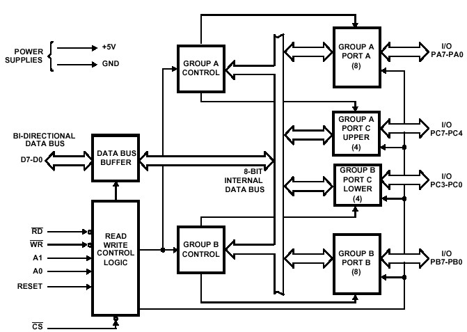
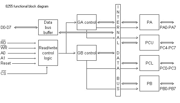
The 8255 PPI chip is a general purpose input/output IC. This document will describe it's role in the Amstrad CPC,CPC+ and KC compact systems. To understand it's full functions please read the datasheet.
In these systems it is connected to the AY-3-8912 Programmable Sound Generator (PSG), keyboard, cassette recorder, the VSYNC of the 6845 CRTC and the "busy" signal from the parallel port.
The PPI is selected when A11 of the I/O port address is set to "0", A9 and A8 then define the PPI function access (as shown below), A15-A12 and A10 should be "1" (to prevent conflicts with other hardware), A7-A0 are don't care. So, resulting Port addresses are:
| I/O address | A9 | A8 | Description | Read/Write status | Used Direction | Used for |
| &F4xx | 0 | 0 | Port A Data | Read/Write | In/Out | PSG (Sound/Keyboard/Joystick) |
| &F5xx | 0 | 1 | Port B Data | Read/Write | In | Vsync/Jumpers/PrinterBusy/CasIn/Exp |
| &F6xx | 1 | 0 | Port C Data | Read/Write | Out | KeybRow/CasOut/PSG |
| &F7xx | 1 | 1 | Control | Write Only | Out | Control |
In the CPC+, the 8255 is integrated into the ASIC. The "emulation" is not complete and some functionality is not available. Please see the "Extra CPC+ documentation" for more information.
- Mode 1 (Strobed Input/Output) and Mode 2 (Bi-Directional Bus), as far as I know, are not used by any program, Mode 0 (Basic Input/Output) is always used.
Port Usage
- NOTE - If you are using the firmware, always return the operating modes and I/O state of the ports used to their settings below. The firmware expects the settings to be the same as given below and may operate incorrectly if they are not.
PPI Port A
Operating system settings:
- I/O Mode 0,
- For writing data to PSG all bits must be set to output,
- for reading data from PSG all bits must be set to input (thereafter, output direction should be restored, for compatibility with the BIOS).
Bit7-0 : PSG databus
PPI Port B
Operating system settings:
- I/O Mode 0,
- Input
| Bit | Description | Usage in CPC | Usage in KC Compact |
| 7 | CAS.IN | Cassette data input | Cassette data input |
| 6 | PRN.BUSY | Parallel/Printer port ready signal | "1" = not ready, "0" = Ready |
| 5 | /EXP(note 6) | Expansion Port /EXP pin | Printer data bit7 |
| 4 | LK4(note 5) | Screen Refresh Rate | Purpose unknown (set to "1") |
| 3 | LK3(note 1) | Manufacturer ID | Purpose unknown (set to "1") |
| 2 | LK2(note 2) | Manufacturer ID | Purpose unknown (set to "0") |
| 1 | LK1(note 3) | Manufacturer ID | Expansion Port /TEST pin |
| 0 | VSYNC | State of VSYNC from 6845. "1" = VSYNC active, "0" = VSYNC inactive |
Note
1. On CPC464,CPC664,CPC6128 and GX4000 this is LK3 on the PCB. On the CPC464+ and CPC6128+ this is LK103 on the PCB. On the KC compact this is "1".
2. On CPC464,CPC664,CPC6128 and GX4000 this is LK2 on the PCB. On the CPC464+ and CPC6128+ this is LK102 on the PCB. On the KC compact this is "0".
3. On CPC464,CPC664,CPC6128 and GX4000 this is LK1 on the PCB. On the CPC464+ and CPC6128+ this is LK101 on the PCB. On the KC compact this is /TEST signal from the expansion port.
4. On the CPC464,CPC664,CPC6128,CPC464+,CPC6128+ and GX4000 bits 3,2 and 1 define the manufacturer name. See below to see the options available. The manufacturer name is defined on the PCB and cannot be changed through software.
5. On the CPC464,CPC664,CPC6128,CPC464+,CPC6128+ and GX4000 bit 4 defines the Screen refresh frequency. "1" = 50Hz, "0" = 60Hz. This is defined on the PCB and cannot be changed with software. On the KC compact bit 4 is "1"
6. This bit is connected to /EXP signal on the expansion port.
- On the KC Compact this bit is used to define bit 7 of the printer data.
- On the CPC, it is possible to use this bit to define bit 7 of the printer data, so a 8-bit printer port is made, with a hardware modification,
- On the CPC this can be used by a expansion device to report it's presence. "1" = device connected, "0" = device not connected. This is not always used by all expansion devices.
Table showing manufacturer name on power-up (CPC and CPC+ only):
| Bit 3 | Bit 2 | Bit 1 | Manufacturer Name |
| 0 | 0 | 0 | Isp |
| 0 | 0 | 1 | Triumph |
| 0 | 1 | 0 | Saisho |
| 0 | 1 | 1 | Solavox |
| 1 | 0 | 0 | Awa |
| 1 | 0 | 1 | Schneider |
| 1 | 1 | 0 | Orion |
| 1 | 1 | 1 | Amstrad |
PPI Port C
Operating system settings:
- upper: I/O Mode 0, lower: I/O mode 0,
- upper: output, lower: output
| Bit | Description | Usage |
| 7 | PSG BDIR | PSG function selection |
| 6 | PSG BC1 | |
| 5 | Cassette Write data | |
| 4 | Cassette Motor Control | set bit to "1" for motor on, or "0" for motor off |
| 3 | Keyboard line | Select keyboard line to be scanned (0-15) |
| 2 | ||
| 1 | ||
| 0 |
PSG function selection:
| Bit 7 | Bit 6 | Function |
| 0 | 0 | Inactive |
| 0 | 1 | Read from selected PSG register |
| 1 | 0 | Write to selected PSG register |
| 1 | 1 | Select PSG register |
PPI Control
...
Programming Examples
1. Using the control byte
- Setting bit 7 of port C to 1,
            LD B,&F7                ;8255 Control port
            LD A,%00001111          ;Bit Set/reset function
            OUT (C),A               ;Send it to 8255
            RET
- Set port A to input, operating in mode 0, port B to output, operating in mode 0 and port C to input, operating in mode 0.
            LD B,&F7                ;8255 Control port
            LD A,%10011001          ;Configuration function
            OUT (C),A               ;Send it to 8255
            RET
2. Using port A/B/C,
In this example, port A is set to output, port B is set to input, and port C is set to output, and they are all operating in mode 0.
We will only be using port A for these examples.
- Reading from port A,
                                    ;Set port A to input

            LD B,&F7                ;8255 Control port
            LD A,%10010010          ;Configuration function
            OUT (C),A               ;Send to 8255

            LD B,&F4                ;Port A port address
            IN E,(C)                ;Get byte from port

                                    ;Register E holds value from port

                                    ;Return port I/O status and operating modes
                                    ;to previous settings.

            LD B,&F7                ;8255 Control port
            LD A,%10000010          ;Configuration function
            OUT (C),A               ;Send to 8255
            RET
- Writing to port A,
                                    ;Set port A to output

                                    ;(Note the next few lines are not necessary
                                    ;as port A is already acting as output, however
                                    ;it is given here just to make the example
                                    ;more understandable)

            LD B,&F7                ;8255 Control port
            LD A,%10000010          ;Configuration function
            OUT (C),A               ;Send to 8255

            LD B,&F4                ;port A port address

                                    ;Register E holds value to put into port

            LD E,&FF                ;Data to put into port
            OUT (C),A               ;Send to port A

                                    ;Return port I/O status and operating modes
                                    ;to previous settings.

            LD B,&F7                ;8255 Control port
            LD A,%10000010          ;Configuration function
            OUT (C),A
            RET

