Difference between revisions of "CRTC"
(→Programming) |
(→Unused clones) |
||
| (52 intermediate revisions by the same user not shown) | |||
| Line 2: | Line 2: | ||
NOTE: This document describes the functionality in terms of the CPC with its separate CRTC and Gate-Array. The Plus has both integrated into the same IC, but could be considered to have two functional blocks, one for CRTC and one for Gate-Array. In this document the term 'Gate-Array' is used, but this also applies to the ASIC. | NOTE: This document describes the functionality in terms of the CPC with its separate CRTC and Gate-Array. The Plus has both integrated into the same IC, but could be considered to have two functional blocks, one for CRTC and one for Gate-Array. In this document the term 'Gate-Array' is used, but this also applies to the ASIC. | ||
| + | |||
| + | <br> | ||
== Overview == | == Overview == | ||
| Line 46: | Line 48: | ||
4. As far as I know, the KC compact used HD6845R only. | 4. As far as I know, the KC compact used HD6845R only. | ||
| + | |||
| + | <br> | ||
== Timings and relating with Z80 instructions count == | == Timings and relating with Z80 instructions count == | ||
| Line 51: | Line 55: | ||
Some informations like : how many Z80 instructions can I fit within a scan line ? Within a screen ? Etc... See http://www.cpcwiki.eu/forum/programming/frame-flyback-and-interrupts/msg25106/#msg25106 | Some informations like : how many Z80 instructions can I fit within a scan line ? Within a screen ? Etc... See http://www.cpcwiki.eu/forum/programming/frame-flyback-and-interrupts/msg25106/#msg25106 | ||
(To be extracted/edited to conform to wiki good practices). | (To be extracted/edited to conform to wiki good practices). | ||
| + | |||
| + | <br> | ||
==Programming== | ==Programming== | ||
| Line 75: | Line 81: | ||
1. The function of these I/O ports is dependant on the CRTC type | 1. The function of these I/O ports is dependant on the CRTC type | ||
| − | 2. | + | 2. The CRTC is not connected to the CPU's RD and WR pins, so the CRTC is not aware of the CPU bus I/O direction. Therefore, if you perform an IN instruction to the select or write functions, it will write data to the CRTC from the current data on the bus. |
| + | |||
| + | <br> | ||
==Addressing== | ==Addressing== | ||
| − | The | + | The video memory address VMA of the [[Gate Array]] is constructed from the CRTC MA and RA signals. |
{|{{Prettytable|width: 700px; font-size: 2em;}} | {|{{Prettytable|width: 700px; font-size: 2em;}} | ||
| − | |''Memory Address | + | |''Video Memory Address''||''Signal source''||''Signal name'' |
|- | |- | ||
|A15||6845||MA13 | |A15||6845||MA13 | ||
| Line 118: | Line 126: | ||
|} | |} | ||
| − | CRTC generates the address, Gate | + | CRTC generates the address, Gate Array reads the data and converts it to pixels based on its current graphics mode and palette. |
CRTC pins RA3, RA4, MA10, MA11 are not connected on CPC. | CRTC pins RA3, RA4, MA10, MA11 are not connected on CPC. | ||
| − | == CUDISP == | + | <br> |
| + | |||
| + | == CUDISP (aka CURSOR) == | ||
| − | CUDISP signal defines the hardware cursor. | + | CUDISP (Cursor Display) signal defines the hardware cursor. |
CRTC pin CUDISP is not connected to the Gate Array, so it has no effect on a barebone CPC or Plus machine. | CRTC pin CUDISP is not connected to the Gate Array, so it has no effect on a barebone CPC or Plus machine. | ||
| Line 130: | Line 140: | ||
However, this signal is provided to the expansion port. And it is used by the [[PlayCity]] and [[Play2CPC]] expansions. | However, this signal is provided to the expansion port. And it is used by the [[PlayCity]] and [[Play2CPC]] expansions. | ||
| − | + | <br> | |
| − | DISPTMG signal defines the border. When DISPTMG is " | + | == DISPTMG (aka Display Enable) == |
| + | |||
| + | DISPTMG (Display Timing) signal defines the border. When DISPTMG is "0" the border colour is output by the Gate Array to the display. | ||
The border has higher priority than pixels but lower priority than the black colour output when HSYNC/VSYNC are active. | The border has higher priority than pixels but lower priority than the black colour output when HSYNC/VSYNC are active. | ||
| − | + | The DISPTMG can be forced to 0 by using R8 (DISPTMG Skew) on type 0,3 and 4 or by setting R6=0 on type 1. It is not possible to force the DISPTMG on type 2. | |
| − | + | <br> | |
| − | + | == HSYNC and VSYNC == | |
| − | + | On CPC, HSYNC and VSYNC from the CRTC are passed to the [[Gate Array]] for further modification. See its wiki page. | |
| − | + | The HSYNC width value is interpreted differently between CRTCs. On CRTCs 0/1, if 0 is programmed no HSYNC is generated. On CRTCs 2/3/4, if 0 is programmed this gives a HSYNC width of 16. | |
| − | + | During an HSYNC, if HSYNC width is changed with a value less than the current HSC, then HSC is overflowing. The only exception is for CRTC 1 with a value of 0, which cancels the current HSYNC. | |
| − | + | CRTCs 1/2 have a fixed VSYNC width value of 16. VSYNC width can be configured with Register 3 on CRTCs 0/3/4. If 0 is programmed this gives 16 lines of VSYNC. | |
| − | + | ||
| − | CRTCs 1 | + | |
The bit 0 of port B of the PPI changes to 1 as soon as the VSYNC signal is produced by the CRTC. | The bit 0 of port B of the PPI changes to 1 as soon as the VSYNC signal is produced by the CRTC. | ||
| + | |||
| + | <br> | ||
== The 6845 Registers == | == The 6845 Registers == | ||
| Line 167: | Line 179: | ||
|2||Horizontal Sync Position ||00000000||46||When to start the HSync signal. | |2||Horizontal Sync Position ||00000000||46||When to start the HSync signal. | ||
|- | |- | ||
| − | |3||Horizontal and Vertical Sync Widths||VVVVHHHH||128+14|| | + | |3||Horizontal and Vertical Sync Widths||VVVVHHHH||128+14||VSync width in scan-lines (Not present on all CRTCs, fixed to 16 lines on these) ; HSync pulse width in characters. |
|- | |- | ||
|4||Vertical Total (-1)||x0000000||38||Height of the screen, in characters. | |4||Vertical Total (-1)||x0000000||38||Height of the screen, in characters. | ||
| Line 234: | Line 246: | ||
So, it's possible to use 32KB screen size (used for [[Programming:Overscan|overscan]]) by setting bits 11 and 10 both to 1 (of Register 12). Bits MA11 and MA10 of the address generated by the CRTC are not written on the address bus to access video memory; settings both bits to 1 is the only way to cause a carry to bit MA12 when address pass over the end of current video page to change the memory address to the next video page. | So, it's possible to use 32KB screen size (used for [[Programming:Overscan|overscan]]) by setting bits 11 and 10 both to 1 (of Register 12). Bits MA11 and MA10 of the address generated by the CRTC are not written on the address bus to access video memory; settings both bits to 1 is the only way to cause a carry to bit MA12 when address pass over the end of current video page to change the memory address to the next video page. | ||
| + | |||
| + | <br> | ||
== CRTC Differences == | == CRTC Differences == | ||
| Line 346: | Line 360: | ||
'''Notes''' | '''Notes''' | ||
| − | |||
| − | |||
* On types 0 and 1, if a Write Only register is read from, "0" is returned. | * On types 0 and 1, if a Write Only register is read from, "0" is returned. | ||
| Line 354: | Line 366: | ||
* See the document "Extra CPC Plus Hardware Information" for more details. | * See the document "Extra CPC Plus Hardware Information" for more details. | ||
| + | |||
| + | <br> | ||
=== Horizontal and Vertical Sync (R3) === | === Horizontal and Vertical Sync (R3) === | ||
| Line 372: | Line 386: | ||
*Bits 7..4 define Vertical Sync Width. If 0 is programmed this gives 16 lines of VSYNC. | *Bits 7..4 define Vertical Sync Width. If 0 is programmed this gives 16 lines of VSYNC. | ||
*Bits 3..0 define Horizontal Sync Width. If 0 is programmed this gives a HSYNC width of 16. | *Bits 3..0 define Horizontal Sync Width. If 0 is programmed this gives a HSYNC width of 16. | ||
| + | |||
| + | <br> | ||
=== Interlace and Skew (R8) === | === Interlace and Skew (R8) === | ||
| Line 386: | Line 402: | ||
| − | + | 2 interlace modes are available: | |
| − | + | * In interlace sync mode, the same information is painted in both fields to enhance readability. In this mode, reprogramming the CRTC is not necessary | |
| + | * In interlace sync and video mode, alternating lines are displayed in the even and odd field to double the resolution. In this mode, it is necessary to reprogram the CRTC as if we were building a frame of 624 lines. The 625th line is managed automatically by the CRTC | ||
[[File:CRTC Interlace modes.png]] | [[File:CRTC Interlace modes.png]] | ||
| − | === | + | <br> |
| + | |||
| + | === R31 on Type 1 === | ||
R31 is described in the UM6845R documentation as "Dummy Register". | R31 is described in the UM6845R documentation as "Dummy Register". | ||
| Line 400: | Line 419: | ||
R31 doesn't exist on types 0,2,3,4. | R31 doesn't exist on types 0,2,3,4. | ||
| − | === | + | <br> |
| + | |||
| + | === R12/R13 on Type 1 === | ||
The UM6845R differs to other CRTC in respect of R12/R13. | The UM6845R differs to other CRTC in respect of R12/R13. | ||
| Line 410: | Line 431: | ||
In demos to make a display compatible with all CRTCs, program R12/R13 when VCC!=0. This will then take effect at the next frame start. | In demos to make a display compatible with all CRTCs, program R12/R13 when VCC!=0. This will then take effect at the next frame start. | ||
| − | === | + | <br> |
| + | |||
| + | === Status register on Type 1 === | ||
The UM6845R has a status register that can be read using port &BExx. | The UM6845R has a status register that can be read using port &BExx. | ||
| Line 422: | Line 445: | ||
All the other bits read as 0 and don't have any function. | All the other bits read as 0 and don't have any function. | ||
| + | |||
| + | <br> | ||
=== R10/R11 on ASIC/Pre-ASIC === | === R10/R11 on ASIC/Pre-ASIC === | ||
| Line 506: | Line 531: | ||
|(C9=R9 and C0=R0) or (C9=0 and C0=0 to R0-1) | |(C9=R9 and C0=R0) or (C9=0 and C0=0 to R0-1) | ||
|} | |} | ||
| + | |||
| + | <br> | ||
=== Reading from CRTC registers on ASIC/Pre-ASIC === | === Reading from CRTC registers on ASIC/Pre-ASIC === | ||
| Line 559: | Line 586: | ||
! Abbr | ! Abbr | ||
! Alternate name | ! Alternate name | ||
| + | ! Comment | ||
|- | |- | ||
|Horizontal Character Counter | |Horizontal Character Counter | ||
|HCC | |HCC | ||
|C0 | |C0 | ||
| + | | | ||
|- | |- | ||
|Horizontal Sync Counter | |Horizontal Sync Counter | ||
|HSC | |HSC | ||
|C3l | |C3l | ||
| + | | | ||
|- | |- | ||
|Vertical Character Counter | |Vertical Character Counter | ||
|VCC | |VCC | ||
|C4 | |C4 | ||
| + | | | ||
|- | |- | ||
|Vertical Sync Counter | |Vertical Sync Counter | ||
| Line 579: | Line 610: | ||
|VLC | |VLC | ||
|C9 | |C9 | ||
| + | |If non-interlace, this counter is exposed on CRTC pins RA0..RA4 | ||
|- | |- | ||
|Vertical Total Adjust Counter | |Vertical Total Adjust Counter | ||
|VTAC | |VTAC | ||
| − | |C5 | + | |C5 |
| + | |This counter does not exist on CRTCs 0/3/4. C9 is reused instead | ||
|- | |- | ||
|Frame Counter | |Frame Counter | ||
|FC | |FC | ||
| − | | | + | | |
| + | |Used to alternate frames in interlace and for CRTC cursor blinking | ||
| + | |- | ||
| + | |Memory Address | ||
| + | |MA | ||
| + | | | ||
| + | |This counter is exposed on CRTC pins MA0..MA13 | ||
|} | |} | ||
No matter its type, the CRTC never buffers its counters. | No matter its type, the CRTC never buffers its counters. | ||
| − | The only value that is saved in a buffer in the CRTC is the video pointer because it is reloaded at each line start. | + | The only value that is saved in a buffer in the CRTC is the video pointer MA because it is reloaded at each line start. The exception is the CRTC 1 for which the MA is reloaded with R12/R13 instead of MA' as long as C4=0. |
<br> | <br> | ||
| Line 619: | Line 658: | ||
* [[AMS40226 (Amstrad)]] aka Type 4 | * [[AMS40226 (Amstrad)]] aka Type 4 | ||
*[[Media:CRTC-5-HD6345.pdf|HD6345 (Hitachi)]] aka Type 5 - Upgraded pin-compatible CRTC chip with advanced functionalities [https://thecheshirec.at/2024/05/07/un-crtc6345-sur-amstrad-cpc/ Upgrading the CPC to HD6345] | *[[Media:CRTC-5-HD6345.pdf|HD6345 (Hitachi)]] aka Type 5 - Upgraded pin-compatible CRTC chip with advanced functionalities [https://thecheshirec.at/2024/05/07/un-crtc6345-sur-amstrad-cpc/ Upgrading the CPC to HD6345] | ||
| + | |||
| + | <br> | ||
== Unused clones == | == Unused clones == | ||
* [[CM607P]] a Bulgarian clone made in Pravetz factory | * [[CM607P]] a Bulgarian clone made in Pravetz factory | ||
| − | * [[EF6845P]] by Thomson Semiconductors | + | * [[Media:EF6845P.pdf|EF6845]] by Thomson Semiconductors |
| − | * [[UM6845E]] by UMC | + | * [[Media:UM6845E-UMC.pdf|UM6845E]] by UMC |
| − | * [[ | + | * [[Media:F6845.pdf|F6845]] by Fairchild |
| − | * [[ | + | * [[Media:Mos 6545-1 crtc.pdf|CRTC 6545]] (MOS, Rockwell, Synertek) is pin-compatible with the 6845 and only has minor differences |
| − | + | ||
* [https://github.com/hoglet67/BeebFpga/blob/dev/src/common/mc6845.vhd BeebFpga] [https://github.com/MiSTer-devel/Amstrad_MiSTer/blob/master/rtl/UM6845R.v MiSTer] [https://opencores.org/websvn/filedetails?repname=System09&path=%2FSystem09%2Ftrunk%2Frtl%2FVHDL%2Fcrtc6845.vhd OpenCores] Verilog/VHDL implementations of the 6845 | * [https://github.com/hoglet67/BeebFpga/blob/dev/src/common/mc6845.vhd BeebFpga] [https://github.com/MiSTer-devel/Amstrad_MiSTer/blob/master/rtl/UM6845R.v MiSTer] [https://opencores.org/websvn/filedetails?repname=System09&path=%2FSystem09%2Ftrunk%2Frtl%2FVHDL%2Fcrtc6845.vhd OpenCores] Verilog/VHDL implementations of the 6845 | ||
| + | |||
| + | <br> | ||
== Tools about CRTC == | == Tools about CRTC == | ||
| Line 634: | Line 676: | ||
* [[File:Shaker26.dsk]] Shaker - Suite of CRTC tests associated with the CPC CRTC compendium (many of them will not work correctly on emulators and that was the purpose of the tests, to help create more compatible emulation) | * [[File:Shaker26.dsk]] Shaker - Suite of CRTC tests associated with the CPC CRTC compendium (many of them will not work correctly on emulators and that was the purpose of the tests, to help create more compatible emulation) | ||
* [[File:Shaker addon.dsk]] Shaker Add-On (Pixel 1 Hard Scroll / Vertical Rupture all Crtc) | * [[File:Shaker addon.dsk]] Shaker Add-On (Pixel 1 Hard Scroll / Vertical Rupture all Crtc) | ||
| + | |||
| + | <br> | ||
== Links == | == Links == | ||
| Line 640: | Line 684: | ||
* [http://www.grimware.org/doku.php/documentations/devices/crtc CRTC documentation from Grimware] | * [http://www.grimware.org/doku.php/documentations/devices/crtc CRTC documentation from Grimware] | ||
* [http://quasar.cpcscene.net/doku.php?id=assem:crtc Quasar CRTC documentation (in french)] | * [http://quasar.cpcscene.net/doku.php?id=assem:crtc Quasar CRTC documentation (in french)] | ||
| + | * [https://pulkomandy.github.io/shinra.github.io/crtc.html Differences between CRTC types] | ||
* [[Media:Dossier Rupture(Gozeur Paradox).pdf]] | * [[Media:Dossier Rupture(Gozeur Paradox).pdf]] | ||
* [[Media:Dossier CRTC(Ramlaid Mortel).pdf]] Les entrailles du CRTC | * [[Media:Dossier CRTC(Ramlaid Mortel).pdf]] Les entrailles du CRTC | ||
* [https://thecheshirec.at/tag/crtc6845/ Leçons CRTC (CheshireCat)] | * [https://thecheshirec.at/tag/crtc6845/ Leçons CRTC (CheshireCat)] | ||
* [[Media:ACCC1.8-EN.pdf]] [[Media:ACCC1.8-FR.pdf]] CPC CRTC Compendium - Latest (04/2024!) document containing in-depth info about CRTC programming on CPC. | * [[Media:ACCC1.8-EN.pdf]] [[Media:ACCC1.8-FR.pdf]] CPC CRTC Compendium - Latest (04/2024!) document containing in-depth info about CRTC programming on CPC. | ||
| + | |||
| + | <br> | ||
==Related pages== | ==Related pages== | ||
Latest revision as of 14:29, 2 July 2024
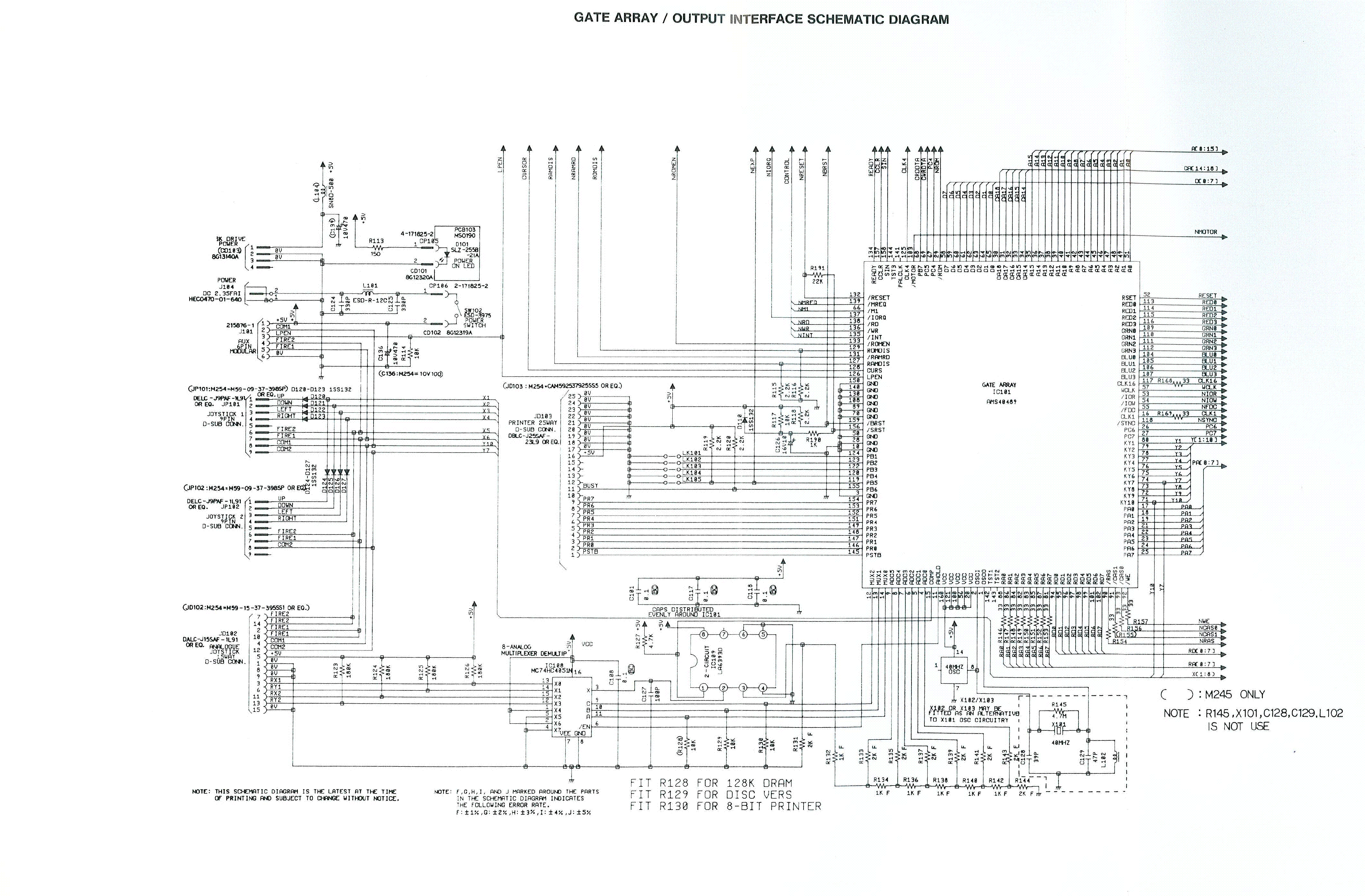
The CRTC (Cathode Ray Tube Controller) helps to generate the video signal of the Amstrad CPC.
NOTE: This document describes the functionality in terms of the CPC with its separate CRTC and Gate-Array. The Plus has both integrated into the same IC, but could be considered to have two functional blocks, one for CRTC and one for Gate-Array. In this document the term 'Gate-Array' is used, but this also applies to the ASIC.
Contents
- 1 Overview
- 2 Timings and relating with Z80 instructions count
- 3 Programming
- 4 Addressing
- 5 CUDISP (aka CURSOR)
- 6 DISPTMG (aka Display Enable)
- 7 HSYNC and VSYNC
- 8 The 6845 Registers
- 9 CRTC Differences
- 10 CRTC Type Detection
- 11 CRTC Timing Diagrams
- 12 Internal Counters
- 13 Hitachi Block Diagram
- 14 UMC Block Diagram
- 15 Motorola Block Diagram
- 16 Datasheets
- 17 Unused clones
- 18 Tools about CRTC
- 19 Links
- 20 Related pages
Overview
The 6845 Cathode Ray Tube Controller (CRTC) is a programmable IC used to generate video displays. This IC is used in a variety of computers including the Amstrad CPC, Amstrad CPC+ and KC Compact.
The CRTC was a common part available from many different manufacturers. During the life of the CPC, Amstrad sourced the CRTC from various manufacturers.
All ICs used were based on the same design but have a different implementation. As a result they do not operate identically in all situations. This document highlights these differences.
This table lists the known ICs used, with their part number, manufacturer and type number.
| Part number | Manufacturer | Type number (note 3) |
| HD6845S | Hitachi | 0 |
| UM6845 | UMC | 0 |
| UM6845R | UMC | 1 |
| MC6845 | Motorola | 2 |
| AMS40489 | Amstrad | 3 (note 1) |
| 40226 | Amstrad | 4 (note 2) |
NOTES
1. The CRTC functionality is integrated into the CPC+ ASIC. This type exists only in the CPC464+,CPC6128+ and GX4000.
2. This type exists in "cost-down" CPC464 and CPC6128 systems. In the "cost-down" the CRTC functionality is integrated into a single ASIC IC. This ASIC is often refered to as the "Pre-ASIC" because it preceeded the CPC+ ASIC. The CRTC functionality of the Pre-ASIC is almost identical to the CRTC within the ASIC.
3. In the Amstrad community each 6845 implementation has been assigned a type number. This type identifies a group of implementations which operate in exactly the same way.
As far as I know, the type number system was originally used by demo programmers.
It is possible to detect the 6845 present using software methods, and this is done to:
- warn that the software was not designed for the detected 6845 and may function incorrectly,
- to adapt the software so that it will run with the detected 6845
- In most cases, the type of the detected 6845 is reported.
4. As far as I know, the KC compact used HD6845R only.
Timings and relating with Z80 instructions count
Some informations like : how many Z80 instructions can I fit within a scan line ? Within a screen ? Etc... See http://www.cpcwiki.eu/forum/programming/frame-flyback-and-interrupts/msg25106/#msg25106 (To be extracted/edited to conform to wiki good practices).
Programming
The 6845 is selected when bit 14 of the I/O port address is set to "0". Bit 9 and 8 of the I/O port address define the function to access. The remaining bits can be any value, but it is adviseable to set these to "1" to avoid conflict with other devices in the system.
The recommended I/O port addresses are
| I/O port address | Function | Read/Write |
| &BCxx | Select 6845 register | Write only |
| &BDxx | Write 6845 register data | Write only |
| &BExx | (note 1) | Read only |
| &BFxx | (note 1) | Read only |
NOTE
1. The function of these I/O ports is dependant on the CRTC type
2. The CRTC is not connected to the CPU's RD and WR pins, so the CRTC is not aware of the CPU bus I/O direction. Therefore, if you perform an IN instruction to the select or write functions, it will write data to the CRTC from the current data on the bus.
Addressing
The video memory address VMA of the Gate Array is constructed from the CRTC MA and RA signals.
| Video Memory Address | Signal source | Signal name |
| A15 | 6845 | MA13 |
| A14 | 6845 | MA12 |
| A13 | 6845 | RA2 |
| A12 | 6845 | RA1 |
| A11 | 6845 | RA0 |
| A10 | 6845 | MA9 |
| A9 | 6845 | MA8 |
| A8 | 6845 | MA7 |
| A7 | 6845 | MA6 |
| A6 | 6845 | MA5 |
| A5 | 6845 | MA4 |
| A4 | 6845 | MA3 |
| A3 | 6845 | MA2 |
| A2 | 6845 | MA1 |
| A1 | 6845 | MA0 |
| A0 | Gate-Array | CCLK |
CRTC generates the address, Gate Array reads the data and converts it to pixels based on its current graphics mode and palette.
CRTC pins RA3, RA4, MA10, MA11 are not connected on CPC.
CUDISP (aka CURSOR)
CUDISP (Cursor Display) signal defines the hardware cursor.
CRTC pin CUDISP is not connected to the Gate Array, so it has no effect on a barebone CPC or Plus machine.
However, this signal is provided to the expansion port. And it is used by the PlayCity and Play2CPC expansions.
DISPTMG (aka Display Enable)
DISPTMG (Display Timing) signal defines the border. When DISPTMG is "0" the border colour is output by the Gate Array to the display.
The border has higher priority than pixels but lower priority than the black colour output when HSYNC/VSYNC are active.
The DISPTMG can be forced to 0 by using R8 (DISPTMG Skew) on type 0,3 and 4 or by setting R6=0 on type 1. It is not possible to force the DISPTMG on type 2.
HSYNC and VSYNC
On CPC, HSYNC and VSYNC from the CRTC are passed to the Gate Array for further modification. See its wiki page.
The HSYNC width value is interpreted differently between CRTCs. On CRTCs 0/1, if 0 is programmed no HSYNC is generated. On CRTCs 2/3/4, if 0 is programmed this gives a HSYNC width of 16.
During an HSYNC, if HSYNC width is changed with a value less than the current HSC, then HSC is overflowing. The only exception is for CRTC 1 with a value of 0, which cancels the current HSYNC.
CRTCs 1/2 have a fixed VSYNC width value of 16. VSYNC width can be configured with Register 3 on CRTCs 0/3/4. If 0 is programmed this gives 16 lines of VSYNC.
The bit 0 of port B of the PPI changes to 1 as soon as the VSYNC signal is produced by the CRTC.
The 6845 Registers
The Internal registers of the 6845 are:
| Register Index | Register Name | Range | CPC Setting | Notes |
| 0 | Horizontal Total (-1) | 00000000 | 63 | Width of the screen, in characters. Should always be 63 (64 characters). 1 character == 1μs. |
| 1 | Horizontal Displayed | 00000000 | 40 | Number of characters displayed. Once horizontal character count (HCC) matches this value, DISPTMG is set to 1. |
| 2 | Horizontal Sync Position | 00000000 | 46 | When to start the HSync signal. |
| 3 | Horizontal and Vertical Sync Widths | VVVVHHHH | 128+14 | VSync width in scan-lines (Not present on all CRTCs, fixed to 16 lines on these) ; HSync pulse width in characters. |
| 4 | Vertical Total (-1) | x0000000 | 38 | Height of the screen, in characters. |
| 5 | Vertical Total Adjust | xxx00000 | 0 | Measured in scanlines, can be used for smooth vertical scrolling on CPC. |
| 6 | Vertical Displayed | x0000000 | 25 | Height of displayed screen in characters. Once vertical character count (VCC) matches this value, DISPTMG is set to 1. |
| 7 | Vertical Sync Position | x0000000 | 30 | When to start the VSync signal, in characters. |
| 8 | Interlace and Skew | CCDDxxII | 0 | CC: Cursor Skew (Only in CRTCs 0, 3 and 4). DD: Display Skew (Only in CRTCs 0, 3 and 4). II: Interlace Mode. |
| 9 | Maximum Raster Address (aka Number of Scan Lines) (-1) | xxx00000 | 7 | Maximum scan line address on CPC can hold between 0 and 7, higher values' upper bits are ignored |
| 10 | Cursor Start Raster | xBP00000 | 0 | Cursor signal is not connected to the Gate Array but is provided to the expansion port. B = Blink On/Off; P = Blink Period Control (Slow/Fast). Sets first raster row of character that cursor is on to invert. |
| 11 | Cursor End Raster | xxx00000 | 0 | Sets last raster row of character that cursor is on to invert |
| 12 | Display Start Address (High) | xx000000 | 48 | On Amstrad Plus, bit7 of the printer port is controlled by bit3 of CRTC R12 (ie. bit11 of Display Start Address) |
| 13 | Display Start Address (Low) | 00000000 | 0 | Allows you to offset the start of screen memory for hardware scrolling, and if using memory from address &0000 with the firmware. |
| 14 | Cursor Address (High) | xx000000 | 0 | |
| 15 | Cursor Address (Low) | 00000000 | 0 | |
| 16 | Light Pen Address (High) | xx000000 | Read Only. On CRTC1, bit6 of Status register goes to 0 when R16 is read | |
| 17 | Light Pen Address (Low) | 00000000 | Read Only. On CRTC1, bit6 of Status register goes to 0 when R17 is read |
registers 18-31 read as 0, on type 0 and 2. registers 18-30 read as 0 on type1, register 31 reads as 0xff.
Details about Reg. 12 and Reg. 13 specifically:
 .------- REG 12 --------.   .------- REG 13 --------.
 |                       |   |                       |
  15 14 13 12 11 10 09 08     07 06 05 04 03 02 01 00
 .--.--.--.--.--.--.--.--.   .--.--.--.--.--.--.--.--.
 |X |X |  |  |  |  |  |  |   |  |  |  |  |  |  |  |  |
 '--'--'--'--'--'--'--'--'   '--'--'--'--'--'--'--'--'
       '--.--'--.--'---------------.-----------------'
          |     |                  |
          |     |                  '------> Offset for setting
          |     |                           videoram
          |     |                           (1024 positions)
          |     |                           Bits 0..9
          |     |
          |     '-------------------------> Video Buffer : note (1)
          |
          '-------------------------------> Video Page : note (2)
 note (1)                 note (2)
 .--.--.--------------.  .--.--.---------------.
 |11|10| Video Buffer |  |13|12|   Video Page  |
 |--|--|--------------|  |--|--|---------------|
 | 0| 0|     16Ko     |  | 0| 0|  0000 - 3FFF  |
 |--|--|--------------|  |--|--|---------------|
 | 0| 1|     16Ko     |  | 0| 1|  4000 - 7FFF  |
 |--|--|--------------|  |--|--|---------------|
 | 1| 0|     16Ko     |  | 1| 0|  8000 - BFFF  |
 |--|--|--------------|  |--|--|---------------|
 | 1| 1|     32Ko     |  | 1| 1|  C000 - FFFF  |
 '--'--'--------------'  '--'--'---------------'
So, it's possible to use 32KB screen size (used for overscan) by setting bits 11 and 10 both to 1 (of Register 12). Bits MA11 and MA10 of the address generated by the CRTC are not written on the address bus to access video memory; settings both bits to 1 is the only way to cause a carry to bit MA12 when address pass over the end of current video page to change the memory address to the next video page.
CRTC Differences
In this section I will attempt to identify all the differences between each CRTC.
The following tables list the functions that can be accessed for each type:
Type 0
| b1 | b0 | Function | Read/Write |
| 0 | 0 | Select internal 6845 register | Write Only |
| 0 | 1 | Write to selected internal 6845 register | Write Only |
| 1 | 0 | - | - |
| 1 | 1 | Read from selected internal 6845 register | Read Only |
Type 1
| b1 | b0 | Function | Read/Write |
| 0 | 0 | Select internal 6845 register | Write Only |
| 0 | 1 | Write to selected internal 6845 register | Write Only |
| 1 | 0 | Read Status Register | Read Only |
| 1 | 1 | Read from selected internal 6845 register | Read Only |
Type 2
| b1 | b0 | Function | Read/Write |
| 0 | 0 | Select internal 6845 register | Write Only |
| 0 | 1 | Write to selected internal 6845 register | Write Only |
| 1 | 0 | - | - |
| 1 | 1 | Read from selected internal 6845 register | Read Only |
Type 3 and 4
| b1 | b0 | Function | Read/Write |
| 0 | 0 | Select internal 6845 register | Write Only |
| 0 | 1 | Write to selected internal 6845 register | Write Only |
| 1 | 0 | Read from selected internal 6845 register | Read Only |
| 1 | 1 | Read from selected internal 6845 register | Read Only |
It is not possible to read from all the internal registers, this table shows the read/write status of each register for each type:
| Register Index | Register Name | Type | ||
| 0 | 1 & 2 | 3 & 4 | ||
| 0 | Horizontal Total (-1) | Write Only | ||
| 1 | Horizontal Displayed | Write Only | ||
| 2 | Horizontal Sync Position | Write Only | ||
| 3 | Horizontal and Vertical Sync Widths | Write Only | ||
| 4 | Vertical Total (-1) | Write Only | ||
| 5 | Vertical Total Adjust | Write Only | ||
| 6 | Vertical Displayed | Write Only | ||
| 7 | Vertical Sync Position | Write Only | ||
| 8 | Interlace and Skew | Write Only | ||
| 9 | Maximum Raster Address (aka Number of Scan Lines) (-1) | Write Only | ||
| 10 | Cursor Start Raster | Write Only | Write Only | Read/Write |
| 11 | Cursor End Raster | Write Only | Write Only | Read/Write |
| 12 | Display Start Address (High) | Read/Write | Write Only | Read/Write |
| 13 | Display Start Address (Low) | Read/Write | Write Only | Read/Write |
| 14 | Cursor Address (High) | Read/Write | ||
| 15 | Cursor Address (Low) | Read/Write | ||
| 16 | Light Pen Address (High) | Read Only | ||
| 17 | Light Pen Address (Low) | Read Only | ||
Notes
- On types 0 and 1, if a Write Only register is read from, "0" is returned.
- CRTC types 3 and 4 are identical in every way, except for the unlocking mechanism, split-screen and 8-bit printer port functionalities specific to the ASIC.
- See the document "Extra CPC Plus Hardware Information" for more details.
Horizontal and Vertical Sync (R3)
Type 0:
- Bits 7..4 define Vertical Sync Width. If 0 is programmed this gives 16 lines of VSYNC.
- Bits 3..0 define Horizontal Sync Width. If 0 is programmed no HSYNC is generated.
Type 1:
- Bits 7..4 are ignored. Vertical Sync is fixed at 16 lines.
- Bits 3..0 define Horizontal Sync Width. If 0 is programmed no HSYNC is generated.
Type 2:
- Bits 7..4 are ignored. Vertical Sync is fixed at 16 lines.
- Bits 3..0 define Horizontal Sync Width. If 0 is programmed this gives a HSYNC width of 16.
Types 3/4:
- Bits 7..4 define Vertical Sync Width. If 0 is programmed this gives 16 lines of VSYNC.
- Bits 3..0 define Horizontal Sync Width. If 0 is programmed this gives a HSYNC width of 16.
Interlace and Skew (R8)
Types 0/3/4:
- Bits 7..6 define the skew (delay) of the CUDISP signal (00 = Non-skew ; 01 = One-character skew ; 10 = Two-character skew ; 11 = Non-output).
- Bits 5..4 define the skew (delay) of the DISPTMG signal (00 = Non-skew ; 01 = One-character skew ; 10 = Two-character skew ; 11 = Non-output).
- Bits 3..2 are ignored.
- Bits 1..0 define the interlace mode (00 = No Interlace; 01 = Interlace Sync; 10 = No Interlace; 11 = Interlace Sync and Video).
Types 1/2:
- Bits 7..2 are ignored.
- Bits 1..0 define the interlace mode.
2 interlace modes are available:
- In interlace sync mode, the same information is painted in both fields to enhance readability. In this mode, reprogramming the CRTC is not necessary
- In interlace sync and video mode, alternating lines are displayed in the even and odd field to double the resolution. In this mode, it is necessary to reprogram the CRTC as if we were building a frame of 624 lines. The 625th line is managed automatically by the CRTC

R31 on Type 1
R31 is described in the UM6845R documentation as "Dummy Register".
Its use is described in the documentation for the Rockwell R6545 in combination with R18, R19 and R8 and the Status Register.
In the UM6845R it appears to have no effect. Reading and writing does nothing. Reading it returns 0x0ff.
R31 doesn't exist on types 0,2,3,4.
R12/R13 on Type 1
The UM6845R differs to other CRTC in respect of R12/R13.
When VCC=0, R12/R13 is re-read at the start of each line. R12/R13 can therefore be changed for each scanline when VCC=0.
Just like other CRTCs when RC==(R9-1), the current MA is captured for the next char-line.
In demos to make a display compatible with all CRTCs, program R12/R13 when VCC!=0. This will then take effect at the next frame start.
Status register on Type 1
The UM6845R has a status register that can be read using port &BExx.
Bit 6 is set to 1 if there is a strobe input to the /LPEN signal. It is cleared to 0 when either R17 or R16 (LPEN address) of the CRTC are read. It signals there is a valid LPEN input. On my CPC (arnoldemu) with UM6845R, it is triggered at power on, R17 and R16 have the values 0 when read.
Bit 5 is set to 1 when CRTC is in "vertical blanking". Vertical blanking is when the vertical border is active. i.e. VCC>=R6.
It is cleared when the frame is started (VCC=0). It is not directly related to the DISPTMG output (used by the CPC to display the border colour) because that output is a combination of horizontal and vertical blanking. This bit will be 0 when pixels are being displayed.
All the other bits read as 0 and don't have any function.
R10/R11 on ASIC/Pre-ASIC
The cursor raster registers R10/R11 act as status registers when read on Types 3 & 4. They behave as normal cursor raster registers upon write.
| R10 - Bit number | Bit value | Event |
|---|---|---|
| 0 | 1 | C0=R0 |
| 1 | 0 | C0=R0/2 |
| 2 | 0 | C0=R1-1 (if R0>=R1) |
| 3 | 0 | C0=R2 |
| 4 | 0 | C0=R2+R3 |
| 5 | 0
1 |
R3h>0 : C0=0..R0 on the line R3h from Vsync (C4=R7)
R3h=0 : C0=0..R0 over 15 lines from Vsync (C4=R7) |
| 6 | 1 | Always 1 |
| 7 | 0
0 |
C0=0..R0-1 : VMA.Lsb=0xFF
C0=R0 : VMA'.Lsb=0x00 (same cond if C0=R0=0) |
| R11 - Bit number | Bit value | Event |
|---|---|---|
| 0 | 0 | C4=R4 and C9=R9 and C0=R0 : Last char of screen |
| 1 | 0 | C4=R6-1 and C9=R9 and C0=R0 : Last char displayed |
| 2 | 0 | C4=R7-1 and C9=R9 and C0=R0 : Last char before Vsync |
| 3 | 0/1 | Timer 16 CRTC frames |
| 4 | 1 | Always 1 |
| 5 | 0 | C9=R9 : C0=0 to R0 |
| 6 | 0 | Always 0 |
| 7 | 1 | (C9=R9 and C0=R0) or (C9=0 and C0=0 to R0-1) |
Reading from CRTC registers on ASIC/Pre-ASIC
On CRTC Types 3 and 4, only the 3 least significant bits of the selected register number are considered to read a register according to the following table:
| Nb | Register | Definition |
| 0 | R16 | Light Pen Address (High) |
| 1 | R17 | Light Pen Address (Low) |
| 2 | R10 | Cursor Start Raster |
| 3 | R11 | Cursor End Raster |
| 4 | R12 | Display Start Address (High) |
| 5 | R13 | Display Start Address (Low) |
| 6 | R14 | Cursor Address (High) |
| 7 | R15 | Cursor Address (Low) |
Therefore, as an example, reading register 4 will give the same result as reading register 12 or 20.
CRTC Type Detection
10 MODE 1:' Reinitialize screen
20 OUT &BC00,31:IF INP(&BF00)=255 THEN PRINT"crtc 1":END
30 OUT &BC00,12:IF INP(&BF00)=0 THEN PRINT"crtc 2":END
40 OUT &BC00,20:IF INP(&BF00)=0 THEN PRINT"crtc 0":END
50 PRINT"crtc 3/4"
CRTC Timing Diagrams


Internal Counters
| Counter name | Abbr | Alternate name | Comment |
|---|---|---|---|
| Horizontal Character Counter | HCC | C0 | |
| Horizontal Sync Counter | HSC | C3l | |
| Vertical Character Counter | VCC | C4 | |
| Vertical Sync Counter | VSC | C3h | |
| Vertical Line Counter | VLC | C9 | If non-interlace, this counter is exposed on CRTC pins RA0..RA4 |
| Vertical Total Adjust Counter | VTAC | C5 | This counter does not exist on CRTCs 0/3/4. C9 is reused instead |
| Frame Counter | FC | Used to alternate frames in interlace and for CRTC cursor blinking | |
| Memory Address | MA | This counter is exposed on CRTC pins MA0..MA13 |
No matter its type, the CRTC never buffers its counters.
The only value that is saved in a buffer in the CRTC is the video pointer MA because it is reloaded at each line start. The exception is the CRTC 1 for which the MA is reloaded with R12/R13 instead of MA' as long as C4=0.
Hitachi Block Diagram

UMC Block Diagram

Motorola Block Diagram

Datasheets
- HD6845S (Hitachi) aka Type 0
- UM6845 (UMC) aka Type 0
- UM6845R (UMC) aka Type 1
- MC6845 (Motorola) aka Type 2 Other datasheet version
- AMS40489 (Amstrad) aka Type 3
- AMS40226 (Amstrad) aka Type 4
- HD6345 (Hitachi) aka Type 5 - Upgraded pin-compatible CRTC chip with advanced functionalities Upgrading the CPC to HD6345
Unused clones
- CM607P a Bulgarian clone made in Pravetz factory
- EF6845 by Thomson Semiconductors
- UM6845E by UMC
- F6845 by Fairchild
- CRTC 6545 (MOS, Rockwell, Synertek) is pin-compatible with the 6845 and only has minor differences
- BeebFpga MiSTer OpenCores Verilog/VHDL implementations of the 6845
Tools about CRTC
- some BASIC tools to detect CRTC types 0-1-2 and show some effects by Elmar Krieger (DSK for Emulators)
- File:Shaker26.dsk Shaker - Suite of CRTC tests associated with the CPC CRTC compendium (many of them will not work correctly on emulators and that was the purpose of the tests, to help create more compatible emulation)
- File:Shaker addon.dsk Shaker Add-On (Pixel 1 Hard Scroll / Vertical Rupture all Crtc)
Links
- Wikipedia on the CRTC
- CRTC documentation from Grimware
- Quasar CRTC documentation (in french)
- Differences between CRTC types
- Media:Dossier Rupture(Gozeur Paradox).pdf
- Media:Dossier CRTC(Ramlaid Mortel).pdf Les entrailles du CRTC
- Leçons CRTC (CheshireCat)
- Media:ACCC1.8-EN.pdf Media:ACCC1.8-FR.pdf CPC CRTC Compendium - Latest (04/2024!) document containing in-depth info about CRTC programming on CPC.
Related pages
- Synchronising with the CRTC and display : technic and details on the relationship between Gate Array and CRTC.