(→ELECTRICAL CHARACTERISTICS (AY-3-8910, AY-3-8912)) |
Executioner (Talk | contribs) (→Amplitude Control (Registers R10,R11,R12): fixed table format) |
||
| (12 intermediate revisions by 3 users not shown) | |||
| Line 12: | Line 12: | ||
== DESCRIPTION == | == DESCRIPTION == | ||
| − | The AY-3-8910/8912/8913 Programmable Sound Generator (PSG) is a LSI Circuit which can produce a wide variety of complex sounds under software control. The AY-3-8910/8912/8913 is manufactured in the General Instrument N-Channel Ion Implant Process. Operation requires a single +5V power supply, a TTL compatible clock, and a microprocessor controller such as the General Instrument 16-bit CP1610 or one of the PIC1650 series of 8-bit microcomputers. | + | The [[AY]]-3-8910/8912/8913 Programmable Sound Generator (PSG) is a LSI Circuit which can produce a wide variety of complex sounds under software control. The AY-3-8910/8912/8913 is manufactured in the General Instrument N-Channel Ion Implant Process. Operation requires a single +5V power supply, a TTL compatible clock, and a microprocessor controller such as the General Instrument 16-bit CP1610 or one of the PIC1650 series of 8-bit microcomputers. |
The PSG is easily interfaced to any bus orientation system, its flexibility makes it useful in applications such as music synthesis, sound effects generation, audible alarms, tone signalling and FSK modems. The analog sound outputs can each provide 4bits of logarithmic digital to analog conversion greatly enhancing the dynamic range of the sounds produced. | The PSG is easily interfaced to any bus orientation system, its flexibility makes it useful in applications such as music synthesis, sound effects generation, audible alarms, tone signalling and FSK modems. The analog sound outputs can each provide 4bits of logarithmic digital to analog conversion greatly enhancing the dynamic range of the sounds produced. | ||
| Line 246: | Line 246: | ||
|colspan=4|NOT USED||TP11||TP10||TP9||TP8||TP7||TP6||TP5||TP4||TP3||TP2||TP1||TP0 | |colspan=4|NOT USED||TP11||TP10||TP9||TP8||TP7||TP6||TP5||TP4||TP3||TP2||TP1||TP0 | ||
|- | |- | ||
| − | |12-bit Tone Period (TP) to Tone Generator | + | |colspan=4| ||colspan=12|12-bit Tone Period (TP) to Tone Generator |
|} | |} | ||
| Line 258: | Line 258: | ||
{|{{Prettytable|width: 700px; font-size: 2em;}} | {|{{Prettytable|width: 700px; font-size: 2em;}} | ||
|- | |- | ||
| − | + | |'''B7'''||'''B6'''||'''B5'''||'''B4'''||'''B3'''||'''B2'''||'''B1'''||'''B0''' | |
|- | |- | ||
|colspan=3|NOT USED||colspan=5|5-bit Noise Period (NP) to Noise Generator | |colspan=3|NOT USED||colspan=5|5-bit Noise Period (NP) to Noise Generator | ||
| Line 304: | Line 304: | ||
|colspan=3|NOT USED||M||L3||L2||L1||L0 | |colspan=3|NOT USED||M||L3||L2||L1||L0 | ||
|- | |- | ||
| − | |colspan=3| ||amplitude "mode"|| | + | |colspan=3| ||amplitude "mode"||colspan=4|4-bit "fixed" amplitude level |
|} | |} | ||
| Line 483: | Line 483: | ||
'''Analogue Channel Output Test Curcuit''' | '''Analogue Channel Output Test Curcuit''' | ||
| + | |||
| + | [[Image:psg11.gif]] | ||
== ELECTRICAL CHARACTERISTICS (AY-3-8913) == | == ELECTRICAL CHARACTERISTICS (AY-3-8913) == | ||
| Line 498: | Line 500: | ||
* Exceeding these ratings could cause permanent damage to the device. This is a stress rating only and functional operation of the devices at these conditions is not implied -- operating ranges are specified in Standard Conditions. Exposure to absolute maximum rating conditions for extended periods may affect device reliability. Data labelled " typical" is presented for design guidance only and is not guaranteed. | * Exceeding these ratings could cause permanent damage to the device. This is a stress rating only and functional operation of the devices at these conditions is not implied -- operating ranges are specified in Standard Conditions. Exposure to absolute maximum rating conditions for extended periods may affect device reliability. Data labelled " typical" is presented for design guidance only and is not guaranteed. | ||
| − | Storage Conditions (unless otherwise noted): | + | '''Storage Conditions (unless otherwise noted):''' |
Vcc = ± 5V ±5% | Vcc = ± 5V ±5% | ||
| Line 506: | Line 508: | ||
Operating Temperature = 0°C to +70°C | Operating Temperature = 0°C to +70°C | ||
| + | {|{{Prettytable|width: 700px; font-size: 2em;}} | ||
| + | |'''Characteristics'''||'''Min'''||'''Sym'''||'''Max'''||'''Units'''||'''Conditions''' | ||
| + | |- | ||
| + | |'''DC CHARACTERISTICS''' | ||
| + | |- | ||
| + | |'''All inputs''' | ||
| + | |- | ||
| + | |Low level||Vil||0||0.7||V | ||
| + | |- | ||
| + | |High level||Vih||2.2||Vcc||V | ||
| + | |- | ||
| + | |'''All Outputs (except Analog Channel Outputs''' | ||
| + | |- | ||
| + | |Low level||Vol||0||0.4||V||1||TTL||Load | ||
| + | |- | ||
| + | |High level||Voh||2.4||Vcc||V||+100pf | ||
| + | |- | ||
| + | |'''Analog Channel Outputs'''||Vo||0||2000||uA||Test Curcuit: Fig 6 | ||
| + | |- | ||
| + | |'''Power Supply Current'''||Icc||-||85||mA | ||
| + | |- | ||
| + | |'''AC CHARACTERISTICS''' | ||
| + | |- | ||
| + | |'''Clock Input'''||Fig 7. | ||
| + | |- | ||
| + | |Frequency||fc||1||2.5||MHz | ||
| + | |- | ||
| + | |Rise Time||tr||-||50||ns | ||
| + | |- | ||
| + | |Fall Time||tf||-||50||ns | ||
| + | |- | ||
| + | |Duty Cycle||-||40||60||% | ||
| + | |- | ||
| + | |'''Bus Signals (BDIR,BC2,BC1)''' | ||
| + | |- | ||
| + | |Associative Delay Time||tao||-||50||ns | ||
| + | |- | ||
| + | |'''Reset'''||Fig. 8 | ||
| + | |- | ||
| + | |Reset Pulse Width||trw||5||-||us | ||
| + | |- | ||
| + | |Reset to Bus Control Delay Time||trb||100||-||ns | ||
| + | |- | ||
| + | |'''A9, A8, DA7--DA0 (Address Mode)'''||Fig 9 | ||
| + | |- | ||
| + | |Address Setup Time tas 300 - ns | ||
| + | |- | ||
| + | |Address Hold Time tah 50 - ns | ||
| + | |- | ||
| + | |DA7--DA0 (Write Mode)'''||Fig. 10 | ||
| + | |- | ||
| + | |Write Data Pulse Width||tdw||1800||-||ns | ||
| + | |- | ||
| + | |Write Data Setup Time||tds||50||-||ns | ||
| + | |- | ||
| + | |Write Data Hold Time||tdh||100||-||ns | ||
| + | |- | ||
| + | |'''DA7--DA0 (Read Mode)'''||Fig. 11 | ||
| + | |- | ||
| + | |Read Data Access Time||tda||-||350||ns | ||
| + | |- | ||
| + | |'''DA7--DA0 (Inactive Mode)''' | ||
| + | |- | ||
| + | |Tristate Delay Time||tts||-||400||ns | ||
| + | |} | ||
| − | |||
| − | |||
| − | |||
| − | |||
| − | |||
| − | |||
| − | |||
| − | |||
| − | |||
| − | |||
| − | |||
| − | |||
| − | |||
| − | |||
| − | |||
| − | |||
| − | |||
| − | |||
| − | |||
| − | |||
| − | |||
| − | |||
| − | |||
| − | |||
| − | |||
| − | |||
| − | |||
| − | |||
| − | |||
| − | |||
| − | |||
| − | |||
| − | |||
| − | |||
| − | |||
| − | |||
| − | |||
| − | |||
| − | |||
| − | |||
| − | |||
| − | |||
| − | |||
| − | |||
| − | |||
| − | |||
| − | |||
| − | |||
| − | |||
| − | |||
| − | |||
| − | |||
| − | |||
| − | |||
| − | |||
| − | |||
| − | |||
| − | |||
| − | |||
| − | + | '''Fig 7. CLOCK AND BUS SIGNAL TIMING''' | |
| − | + | '''Fig 8. RESET TIMING''' | |
| − | Fig | + | '''Fig 9. LATCH ADDRESS TIMING''' |
| − | Fig | + | '''Fig 10. WRITE DATA TIMING''' |
| − | Fig | + | '''Fig 11. READ DATA TIMING''' |
| − | + | ==Links== | |
| − | + | [[AY|AY's page with less specific subjects]] | |
| − | [[Category: | + | [[Category:Electronic Component]] [[Category:Datasheet]][[Category:Music and sound|*]][[Category:CPC Internal Components]] |
Latest revision as of 21:58, 13 March 2011
General Instruments - AY-3-8910, AY-3-8912, AY-3-8913 Programmable Sound Generator
FEATURES
- Full Software Control of Sound Generation
- Interface to Most 8-bit and 16-bit Microprocessors
- Three independantly Programmed Analog Outputs
- Two 8-bit General Purpose I/O ports (AY-3-8910)
- One 8-bit General Purpose I/O port (AY-3-8912)
- Single +5 Volt Supply
DESCRIPTION
The AY-3-8910/8912/8913 Programmable Sound Generator (PSG) is a LSI Circuit which can produce a wide variety of complex sounds under software control. The AY-3-8910/8912/8913 is manufactured in the General Instrument N-Channel Ion Implant Process. Operation requires a single +5V power supply, a TTL compatible clock, and a microprocessor controller such as the General Instrument 16-bit CP1610 or one of the PIC1650 series of 8-bit microcomputers.
The PSG is easily interfaced to any bus orientation system, its flexibility makes it useful in applications such as music synthesis, sound effects generation, audible alarms, tone signalling and FSK modems. The analog sound outputs can each provide 4bits of logarithmic digital to analog conversion greatly enhancing the dynamic range of the sounds produced.
In order to perform sound effects while allowing the processor to continue its other tasks, the PSG can continue to produce sound after the initial commands have been given by the control processor. The fact that realistic sound production often involves more than one effect is satisfied by the three independantly controllable channels available in the PSG.
All of the circuit control signals are digital in nature and intended to be provided directly by a microprocessor/microcomputer. This means that one PSG can produce the full range of required sounds with no change in external circuitry. Since the frequency response of the PSG ranges from sub-audible at its lowest frequency to post-audible at its highest frequency, there are few sounds which are beyond reproduction ith only the simplest electical connections.
Since most applications of a microprocessor/PSG system would also require interfacing between the outside world and the microprocessor, this facility has been designed into the PSG. The AY-3-8910 has two general purpose 8-bit I/O ports and is supplied in a 40 lead package; the AY-3-8912 has one port and 28 leads; the AY-3-8913 has no ports and 24-leads.
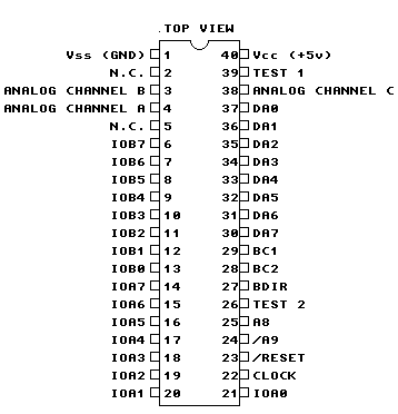
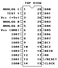
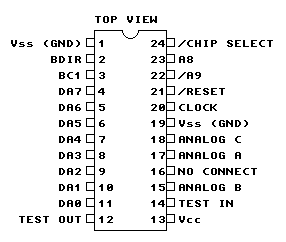
PIN CONFIGURATIONS
PIN FUNCTIONS
DA7--DA0 (input/output/high impedance) pins 30--37 (AY-3-8910) pins 21--28 (AY-3-8912) pins 4--11 (AY-3-8913)
Data/Address 7--0:
These 8 lines comprise the 8-bit bidirectional bus used by the microprocessor to send both data and addresses to the PSG and to recieve data from the PSG. In the data mode, DA7--DA0 correspond to Register Array bits B7--B0. In the address mode, DA3--DA0 select the register number (0--17 8) and a DA7-DA4 in conjunction with address inputs /A9 and A8 for the high order address (chip select).
A8 (input): pin 25 (AY-3-8910) pin 17 (AY-3-8912) pin 23 (AY-3-8913)
/A9 (input): pin 24 (AY-3-8910) pin 28 (AY-3-8912) (not provided on AY-3-8913)
/Address 9,Address 8
These "extra" address bits are made available to enable the positioning of the PSG (assigning a 16 word memory space) in a total 1,024 word memory area rather than in a 256 word memory area as defined by address bits DA7--DA0 alone. If the memory size does not require the use of these extra address lines they may be left unconnected as each is provided with either an on-chip pull down (/A9) or pull-up (A8) resistor. In "noisy" environments, however, it is recommended that /A9 and A8 be tied to an external ground and +5V, respectively, if they are not to be used.
/RESET (input): pin 23 (AY-3-8910) pin 21 (AY-3-8913) pin 16 (AY-3-8912)
For initialization/power on purposes, applying a logic "0" (ground) to the /Reset pin will reset all registers to "0". The /Reset pin is provided with an on-chip pull-up resistor.
CLOCK (signal): pin 22 (AY-3-8910) pin 20 (AY-3-8913) pin 15 (AY-3-8912)
This TTL-compatible input supplies the timing reference for the Tone, Noise and Envelope Generators.
BDIR,BC2,BC1 (inputs): pins 27,28,29 (AY-3-8910) pins 18,19,20 (AY-3-8912) pins 2,3 (No BC2 on AY-3-8913 see below)
Bus DiRection, Bus Control 2,1
These bus control signals are generated directly by the CP1610 series of microprocessors to control all external and internal bus operations in the PSG. When using a processor other than the Cp1610, these signals can be provided either by comparable bus signals or by simulating the signals on I/O lines of the processor. The PSG decodes these signals as illustrated in the following:
| BDIR | BC2 | BC1 | CP1610 Function | PSG Function |
| 0 | 0 | 0 | NACT | INACTIVE. See 010 (IAB) |
| 0 | 0 | 1 | ADAR | LATCH ADDRESS. See 111 (INTAK) |
| 0 | 1 | 0 | IAB | INACTIVE: The PSG/CPU bus is inactive, DA7--DA0 are in high impedence state |
| 0 | 1 | 1 | DTB | READ FROM PSG. This signal causes the contents of the register which is currently addressed to appear on the PSG/CPU bus. DA7--DA0 are in output mode. |
| 1 | 0 | 0 | BAR | LATCH ADDRESS. See 111 (INTAK) |
| 1 | 0 | 1 | DW | INACTIVE. See 010 (IAB) |
| 1 | 1 | 0 | DWS | WRITE TO PSG. This signal indicates that the bus contains register data which should be latched into the currently addressed register DA7--DA0 are in input mode. |
| 1 | 1 | 1 | INTAK | LATCH ADDRESS. This signal indicates that the bus contains a register address which should be latched in the PSG. DA7--DA0 are in the input mode. |
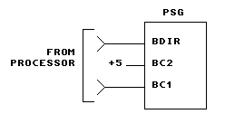
While interfacing to a processor other than the CP1610 would simply require simulating the above decoding, the redundancies in the PSG function vs bus control signals can be used to advantage in that only four of the eight possible decoded bus functions are required by the PSG. This could simpify the programming of the bus control signals to the following, which only require that the processor generate two bus control signals (BDIR and BC1, with BC2 tied to +5v). This is the case with the AY-3-8913 with BC2 pulled high internally.
| BDIR | BC2 | BC1 | PSG Function |
| 0 | 1 | 0 | INACTIVE |
| 0 | 1 | 1 | READ FROM PSG |
| 1 | 1 | 0 | WRITE TO PSG |
| 1 | 1 | 1 | LATCH ADDRESS |
ANALOG CHANNEL A,B,C (outputs): pins 4,3,38 (AY-3-8910) pins 5,4,1 (AY-3-8912) pins 17,15,18 (AY-3-8913)
Each of these signals is the output of its corresponding D/A Converter, and provides a up to 1V peak-peak signal representing the complex sound waveshape generated by the PSG.
IOA7--IOA0 (input/output): pins 14--21 (AY-3-8910) pins 7--14 (AY-3-8912) (not provided on AY-3-8913)
IOB7--IOB0 (input/output): pins 6--13 (AY-3-8910) (not provided on AY-3-8912) (not provided on AY-3-8913)
Input/Output A7--A0, B7--B0
Each of these two parallel input/output ports provides 8 bits of parallel data to/from the PSG/CPU bus from/to any external devices connected to the IOA or IOB pins. Each pin is provided with an on-chip pull-up resistor, so that when in the "input" mode, all pins will read normally high. Therefore, the recommended method for scanning external switches would be to ground the input bit.
TEST 1: pin 39 (AY-3-8910) pin 14 (AY-3-8913) pin 2 (AY-3-8912)
TEST 2: pin 26 (AY-3-8910) pin 12 (AY-3-8913) (not connected on AY-3-8912)
These pins are for General Instrument test purposes only and should be left open -- do not use as tie-points.
Vcc: pin 40 (AY-3-8910) pin 13 (AY-3-8913) pin 3 (AY-3-8912)
Nominal +5Volt power supply to PSG.
Vss: pin 1 (AY-3-8910) pin 19 (AY-3-8913) pin 6 (AY-3-8912)
Ground reference for the PSG.
/CHIP SELECT (Input): pin 24 (AY-3-8913 only)
This input signal goes low to enable the PSG to read data on the data bus or write data from the data bus to one of the internal registers. For these above operations to occur, this signal must be true in addition to the current bus address being a valid PSG address. This signal must be valid for all read and write operations. This pin has an internal pull down to Vss.
ARCHITECTURE
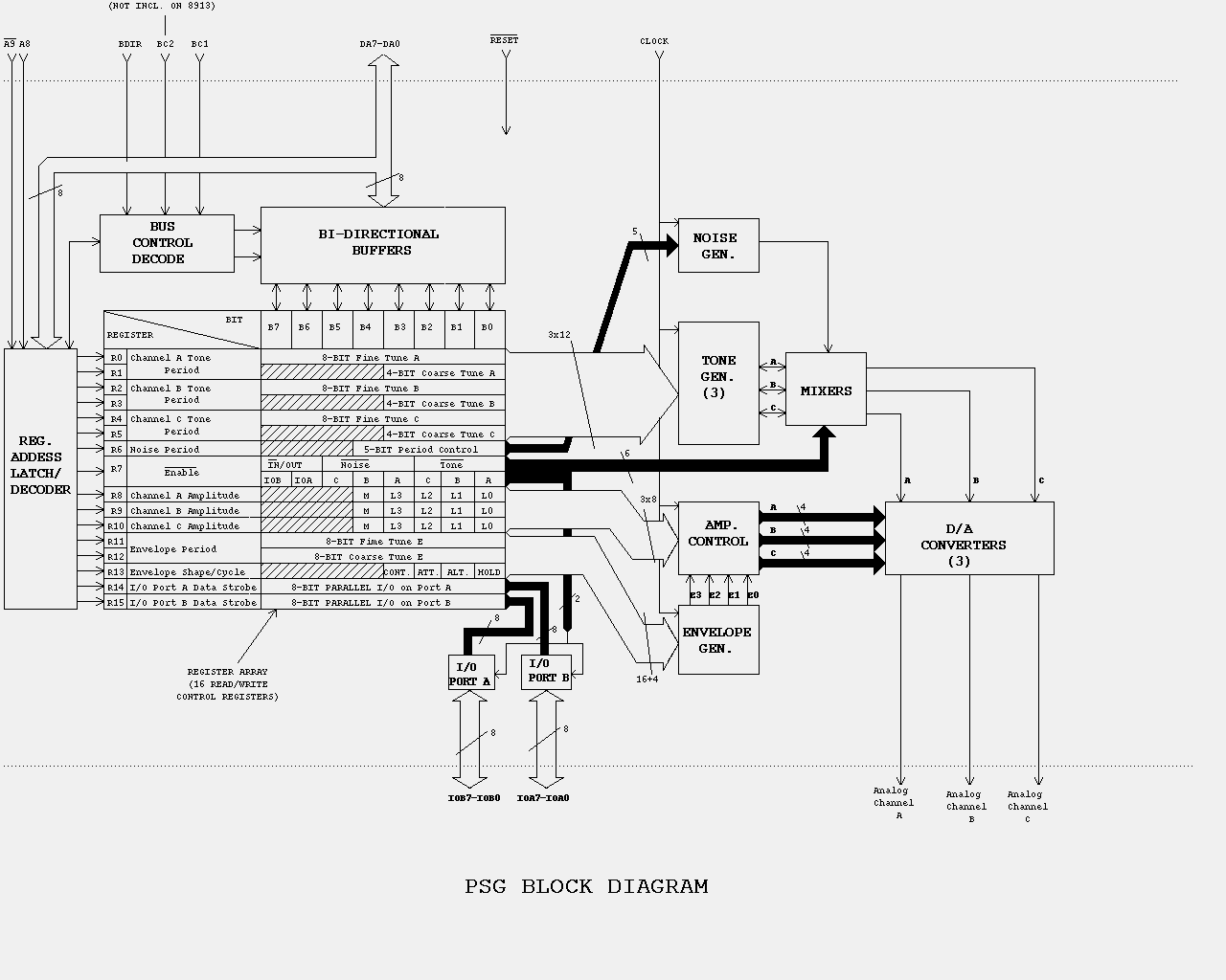
The AY-3-8910/8912/8913 is a register oriented Programmable Sound Generator (PSG). Communication between the processor and the PSG is based on the concept of memory-mapped I/O. Control commands are issued to the PSG by writing to 16 memory-mapped registers. Each of the 16 registers within the PSG is also readable so that the microprocessor can determine, as necessary, present states or stored data values.
All functions of the PSG are controlled through the 16 registers which once programmed, generate and sustain the sounds, thus freeing the system processor for other tasks.
REGISTER ARRAY
The principle element of the PSG is the array of 16 read/write control registers. These 16 registers look to the CPU as a block of memory and as such occupy a 16 word block out of 1,024 possible addresses. The 10 address bits (8 bits on the common data/address bus, and 2 seperate address bits A8 and /A9) are decoded as follows:
| /A9* | A8 | DA7 | DA6 | DA5 | DA4 | DA3 | DA2 | DA1 | DA0 |
| 0 | 1 | 0 | 0 | 0 | 0 | 0 | 0 | 0 | 0 |
THRU
| 0 | 1 | 0 | 0 | 0 | 0 | 1 | 1 | 1 | 1 |
| High Order (Chip Select) | Low order (Register No.) | ||||||||
- /A9 is not provided on the AY-3-8912
The four low order address bits select one of the 16 registers (R0--R17). The six high order address bits function as "chip selects" to control the tri-state bidirectional buffers (when the high order address bits are "incorrect", the bi-directional buffers are forced to the high impedance state). High order address bits /A9, A8 are fixed in the PSG design to recognise a 01 code; high order address bits DA7-DA4 may be mask programmed to any 4-bit code by a special order factory mask modification. Unless otherwise specified, address bits DA7--DA4 are programmed to recognise only a 0000 code. A valid high order address latches the register address (the low order 4 bits) in the Register Address Latch/Decoder block. A latched address will remain valid until the receipt of a new address, enabling multiple reads and writes of the same register contents without the need for redundant re-addressing.
Conditioning of the Register Address Latch/Decoder and the Bidirectional Buffers to recognise the bus function required (inactive, latch address, write data, or read data) is accomplished by the Bus Control Decode block.
SOUND GENERATING BLOCKS
The basic blocks in the PSG which produce the programmed sounds include:
- Tone Generators produce the basic square wave tone frequencies for each channel (A,B,C)
- Noise Generator produces a frequency modulated pseudo random pulse width square wave output.
- Mixers combine the outputs of the Tone Generators and the Noise Generator. One for each channel (A,B,C)
- Amplitude Control provides the D/A Converters with either a fixed or variable amplitude pattern. The fixed amplitude is under direct CPU control; the variable amplitude is accomplished by using, the output of the Envelope Generator.
- Envelope Generator produces an evelope pattern which can be used to amplitude modulate the output of each Mixer.
- D/A Converters the three D/A Converters each produce up to a 16 level output signal as determined by the Amplitude Control.
I/O PORTS
Two additional blocks are shown in the PSG Block Diagram which have nothing directly to do with the production of sound -- these are the two I/O ports (A and B). Since virtually all uses of microprocessor-based sound would require interfacing between the outside world and the processor, this facility has been included in the PSG. Data to/from the CPU bus may be read/written to either of two 8-bit I/O Ports without affecting any other function of the PSG. The I/O Ports are TTL-compatible and are provided with internal pull-ups on each pin. Both Ports are available on the AY-3-8910; only I/O Port A is available on the AY-3-8912; no ports are available on the AY-3-8913.
PSG BLOCK DIAGRAM
OPERATION
Since all functions of the PSG are controlled by the processor via a series of register loads, a detailed description of the PSG operation can best be acomplished by relating each PSG function to the control of its corresponding register. The function of creating or programming a specific sound or sound effect logically follows the control sequence listed:
| Registers|Function | ||
| Tone Generator Control | R0--R5 | Program tone periods. |
| Noise Generator Control | R6 | Program noise period. |
| Mixer Control | R7 | Enable tone and/or noise on selected channels. |
| Amplitude Control | R10--R12 | Select "fixed" or "envelope-variable" amplitudes. |
| Envelope Generator Control | R13--R15 | Program envelope period and select envelope pattern. |
Tone Generator Control (Registers R0,R1,R2,R3,R4,R5)
The frequency of each square wave generated by the three Tone Generators (one each for Channels A,B and C) is obtained in the PSG by first counting down the input clock by 16, then by furthur counting down the result by the programmed 12-bit Tone Period value. Each 12-bit value is obtained in the PSG by combining the contents of the relative Course and Fine Tune registers, as illustrated in the following:
| Course Tone Register | Channel | Fine Tune Register |
| R1 | A | R0 |
| R3 | B | R2 |
| R5 | C | R4 |
| Course Tone Register | Fine Tune Register | ||||||||||||||
| B7 | B6 | B5 | B4 | B3 | B2 | B1 | B0 | B7 | B6 | B5 | B4 | B3 | B2 | B1 | B0 |
| NOT USED | TP11 | TP10 | TP9 | TP8 | TP7 | TP6 | TP5 | TP4 | TP3 | TP2 | TP1 | TP0 | |||
| 12-bit Tone Period (TP) to Tone Generator | |||||||||||||||
Noise Generator Control (Register R6)
The frequency of the noise source is obtained in the PSG by first counting down the input clock by 16, then by furthur counting down the result by the programmed 5-bit Noise Period value. This 5-bit value consists of the lower 5-bits (B4--B0) of register R6, as illustrated in the following:
Noise Period Register
| B7 | B6 | B5 | B4 | B3 | B2 | B1 | B0 |
| NOT USED | 5-bit Noise Period (NP) to Noise Generator | ||||||
Mixer Control Enable (Register R7)
Register R7 is multi-function /Enable register which controls the three Noise/Tone Mixers and the two general purpose I/O Ports.
The Mixers, as previously described, combine the noise and tone frequencies for each of the three channels. The determination of combining neither/either/both noise and tone frequencies on each channel is made by the state of bits B5--B0 of R7.
The direction (input or output) of the two general purpose I/O Ports (IOA and IOB) is determined by the state of bits B7 and B6 of R7.
These functions are illustrated in the following:
Mixer Control-I/O-Enable Register R7
| B7 | B6 | B5 | B4 | B3 | B2 | B1 | B0 |
| /Input Enable | /Noise Enable | /Tone Enable | |||||
| B | A | C | B | A | C | B | A |
Amplitude Control (Registers R10,R11,R12)
The amplitudes of the signals generated by each of the three D/A Converters (one each for Channels A,B and C) is determined by the contents of the lower 5-bits (B4--B0) of registers R10,R11 and R12 as illustrated in the following:
| Amplitude Control Register | Channel |
| R10 | A |
| R11 | B |
| R12 | C |
| B7 | B6 | B5 | B4 | B3 | B2 | B1 | B0 |
| NOT USED | M | L3 | L2 | L1 | L0 | ||
| amplitude "mode" | 4-bit "fixed" amplitude level | ||||||
Envelope Generator Control (Registers R13,R14 and R15)
To acomplish the generation of fairly complex envelope patterns, two independant methods of control are provided in the PSG: first, it is possible to vary the frequency of the envelope using registers R13 and R14; and second, the relative shape and cycle pattern of the envelope can be varied using register R15. The following paragraphis explain the details of the envelope control functions, describing first the envelope period control and then the envelope shape/cycle control.
ENVELOPE PERIOD CONTROL (Registers R13,R14)
The frequency of the envelope is obtained in the PSG by first counting down the input clock by 256, then by furthur counting down the result of the programmed 16-bit Envelope Period value. This 16-bit value is obtained in the PSG by combining the contents of the Envelope Coarse and Fine Tune registers, as illustrated in the following:
| Envelope Coarse Tune Register R14 | Envelope Fine Tune Register R13 | ||||||||||||||
| B7 | B6 | B5 | B4 | B3 | B2 | B1 | B0 | B7 | B6 | B5 | B4 | B3 | B2 | B1 | B0 |
| EP15 | EP14 | EP13 | EP12 | EP11 | EP10 | EP9 | EP8 | EP7 | EP6 | EP5 | EP4 | EP3 | EP2 | EP1 | EP0 |
| 16-bit Envelope Period (EP) to Envelope Generator | |||||||||||||||
ENVELOPE SHAPE/CYCLE CONTROL (Register R15)
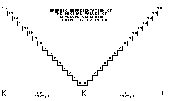
The Envelope Generator furthur counts down the envelope frequency by 16, producing a 16-state per cycle envelope pattern as defined by its 4-bit counter output, E3 E2 E1 E0. The particular shape and cycle pattern of any desired envelope is accomplished by controlling the count pattern (count up/count down) of the 4-bit counter and by defining a single cycle or repeat-cycle pattern.
This envelope shape/cycle control is contained in the 4 bits (B3--B0) of register R15. Each of these 4 bits controls a function in the envelope generator, as illustrated in the following:
Envelope Shape/Cycle Control Register (R15)
| B7 | B6 | B5 | B4 | B3 | B2 | B1 | B0 |
| NOT USED | Hold | Alternate | Attack | Continue | |||
| Function (To Envelope Generator) | |||||||
I/O Port Data Store (Registers R16, R17)
Registers R16 and R17 function as intermediate data storage registers between the PSG/CPU data bus (DA0--DA7) and the two I/O ports (IOA7--IOA0 and IOB7--IOB0). Both ports are available in the AY-3-8910; only I/O port A is available in the AY-3-8912; none are available on the AY-3-8913. Using registers R16 and R17 for the transfer of I/O data has no effect on sound generation.
D/A Converter Operation
Since the primary use of the PSG is to produce sound for the highly imperfect amplitude detection mechanism of the human ear, the D/A conversion is performed in logarithmic steps with a normalized voltage range of from 0 to 1 Volt. The specific amplitude control of each of the three D/A Converters is acomplished by the three sets of 4-bit outputs of the Amplitude Control block, while the Mixer outputs provide the base signal frequency (Noise and/or Tone).
Fig 1. ENVELOPE SHAPE/CYCLE OPERATION
| R15 Bits | GRAPHICAL REPRESENTATION OF ENVELOPE GENERATOR OUTPUT (E3 E2 E1 E0) | |||
| B3 | B2 | B1 | B0 | |
| Continue | Attack | Alternate | Hold | |
| 0 | 0 | x | x | |
| 0 | 1 | x | x | |
| 1 | 0 | 0 | 0 | |
| 1 | 0 | 0 | 1 | |
| 1 | 0 | 1 | 0 | |
| 1 | 0 | 1 | 1 | |
| 1 | 1 | 0 | 0 | |
| 1 | 1 | 0 | 1 | |
| 1 | 1 | 1 | 0 | |
| 1 | 1 | 1 | 1 | |
Fig 2. DETAIL OF TWO CYCLES Of Fig 1 (ref. waveform "1010" in Fig.1)
Fig 3. D/A CONVERTER OUTPUT
Fig 4. SINGLE TONE WITH ENVELOPE SHAPE/CYCLE PATTERN 1010
Fig 5. MIXTURE OF THREE TONES WITH FIXED AMPLITUDE
ELECTRICAL CHARACTERISTICS (AY-3-8910, AY-3-8912)
Maximum Ratings*
Storage Temperature ...... -55°C to +150°C
Operating Temperature ...... 0°C to 40°C
Vcc and all other input/Output Voltages with Respect to Vss ...... -0.3V to +8.0V
Exceeding these ratings could cause permanent damage to the device. This is a stress rating only and functional operation of the devices at these conditions is not implied -- operating ranges are specified in Standard Conditions. Exposure to absolute maximum rating conditions for extended periods may affect device reliability. Data labelled " typical" is presented for design guidance only and is not guaranteed.
Storage Conditions (unless otherwise noted):
Vcc = ± 5V ±5%
Vss = GND
Operating Temperature = 0°C to +40°C
| Characteristics | Sym | Min | Typ** | Max | Units | Conditions |
| DC CHARACTERISTICS | ||||||
| All inputs | ||||||
| Low level | Vil | 0 | - | 0.6 | V | |
| High level | Vih | 2.4 | - | Vcc | V | |
| All Outputs (except Analog Channel Outputs | ||||||
| Low level | Vol | 0 | - | 0.5 | V | Iol = 1.6mA, 20pF |
| High level | Voh | 2.4 | - | Vcc | V | Ioh = 100uA, 20pF |
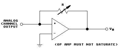
| Analog Channel Outputs | Vo | 0 | - | 60 | dB | Test Curcuit: Fig 6 |
| Power Supply Current | Icc | - | 45 | 85 | mA | |
| AC CHARACTERISTICS | ||||||
| Clock Input | Fig 7. | |||||
| Frequency | fc | 1 | - | 2 | MHz | |
| Rise Time | tr | - | - | 50 | ns | |
| Fall Time | tf | - | - | 50 | ns | |
| Duty Cycle | - | 25 | 50 | 85 | % | |
| Bus Signals (BDIR,BC2,BC1) | ||||||
| Associative Delay Time | tao | - | - | 50 | ns | |
| ResetFig. 8 | ||||||
| Reset Pulse Width | trw | 500 | - | - | ns | |
| Reset to Bus Control Delay Time | trb | 100 | - | - | ns | |
| A9, A8, DA7--DA0 (Address Mode) | Fig 9 | |||||
| Address Setup Time | tas | 400 | - | - | ns | |
| Address Hold Time | tah | 100 | - | - | ns | |
| DA7--DA0 (Write Mode) | Fig. 10 | |||||
| Write Data Pulse Width | tdw | 500 | - | 10,000 | ns | |
| Write Data Setup Time | tds | 50 | - | - | ns | |
| Write Data Hold Time | tdh | 100 | - | - | ns | |
| DA7--DA0 (Read Mode) | Fig. 11 | |||||
| Read Data Access Time | tda | - | 250 | 500 | ns | |
| DA7--DA0 (Inactive Mode) | ||||||
| Tristate Delay Time | tts | - | 100 | 200 | ns |
- Typical values are at ±25°C and nominal voltages
Analogue Channel Output Test Curcuit
ELECTRICAL CHARACTERISTICS (AY-3-8913)
Maximum Ratings*
Storage Temperature ...... -55°C to +150°C
Operating Temperature ...... 0°C to 70°C
Vcc and all other input/Output Voltages with Respect to Vss ...... -0.3V to +8.0V
- Exceeding these ratings could cause permanent damage to the device. This is a stress rating only and functional operation of the devices at these conditions is not implied -- operating ranges are specified in Standard Conditions. Exposure to absolute maximum rating conditions for extended periods may affect device reliability. Data labelled " typical" is presented for design guidance only and is not guaranteed.
Storage Conditions (unless otherwise noted):
Vcc = ± 5V ±5%
Vss = GND
Operating Temperature = 0°C to +70°C
| Characteristics | Min | Sym | Max | Units | Conditions | ||
| DC CHARACTERISTICS | |||||||
| All inputs | |||||||
| Low level | Vil | 0 | 0.7 | V | |||
| High level | Vih | 2.2 | Vcc | V | |||
| All Outputs (except Analog Channel Outputs | |||||||
| Low level | Vol | 0 | 0.4 | V | 1 | TTL | Load |
| High level | Voh | 2.4 | Vcc | V | +100pf | ||
| Analog Channel Outputs | Vo | 0 | 2000 | uA | Test Curcuit: Fig 6 | ||
| Power Supply Current | Icc | - | 85 | mA | |||
| AC CHARACTERISTICS | |||||||
| Clock Input | Fig 7. | ||||||
| Frequency | fc | 1 | 2.5 | MHz | |||
| Rise Time | tr | - | 50 | ns | |||
| Fall Time | tf | - | 50 | ns | |||
| Duty Cycle | - | 40 | 60 | % | |||
| Bus Signals (BDIR,BC2,BC1) | |||||||
| Associative Delay Time | tao | - | 50 | ns | |||
| Reset | Fig. 8 | ||||||
| Reset Pulse Width | trw | 5 | - | us | |||
| Reset to Bus Control Delay Time | trb | 100 | - | ns | |||
| A9, A8, DA7--DA0 (Address Mode) | Fig 9 | ||||||
| Address Setup Time tas 300 - ns | |||||||
| Address Hold Time tah 50 - ns | |||||||
| DA7--DA0 (Write Mode) | Fig. 10 | ||||||
| Write Data Pulse Width | tdw | 1800 | - | ns | |||
| Write Data Setup Time | tds | 50 | - | ns | |||
| Write Data Hold Time | tdh | 100 | - | ns | |||
| DA7--DA0 (Read Mode) | Fig. 11 | ||||||
| Read Data Access Time | tda | - | 350 | ns | |||
| DA7--DA0 (Inactive Mode) | |||||||
| Tristate Delay Time | tts | - | 400 | ns |
Fig 7. CLOCK AND BUS SIGNAL TIMING
Fig 8. RESET TIMING
Fig 9. LATCH ADDRESS TIMING
Fig 10. WRITE DATA TIMING
Fig 11. READ DATA TIMING
