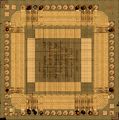
The ACID (Amstrad Cartridge Identification Device) protection chip is used in the cartridges of the Plus series and the GX4000 game console. After Nocash decrypted the internal algorithms it is possible to replace the protection chip with a complex programmable logic device (CPLD).
Technical
The 16pin ACID chip (in the cartridge) is sending a serial data stream to the 160pin ASIC chip (in the computer). The data stream is generated by some shift/xor logic, and is also affected by the EPROM address/enable signals. If the data stream isn't correct, then the ASIC does scatter access to RAM, making the cartridge unusable.
;ACID reverse-engineered 13-16 February 2010 by nocash (Martin Korth)
;below is repeated on every CLK cycle...
CmpVal=13596h, XorVal=0c820h
if PinA0=1 then CmpVal=CmpVal XOR 0000ch, XorVal=XorVal XOR 00004h
if PinA1=1 then CmpVal=CmpVal XOR 06000h, XorVal=XorVal XOR 06000h
if PinA2=1 then CmpVal=CmpVal XOR 000c0h, XorVal=XorVal XOR 00080h
if PinA3=1 then CmpVal=CmpVal XOR 00030h, XorVal=XorVal XOR 00020h
if PinA4=1 then CmpVal=CmpVal XOR 18000h, XorVal=XorVal XOR 08000h
if PinA5=1 then CmpVal=CmpVal XOR 00003h, XorVal=XorVal XOR 00000h
if PinA6=1 then CmpVal=CmpVal XOR 00600h, XorVal=XorVal XOR 00000h
if PinA7=1 then CmpVal=CmpVal XOR 01800h, XorVal=XorVal XOR 00800h
if PinCE=0 AND (ShiftReg OR 100h)=CmpVal then ShiftReg=ShiftReg XOR XorVal
NewBit=ShiftRegBit0 XOR ShiftRegBit9 XOR ShiftRegBit12 XOR ShiftRegBit16
ShiftReg=(ShiftReg SHR 1) + (NewBit SHL 16)
Wait for falling edge on PinCLK
if PinCCLR=0 then ShiftReg=1FFFFh      ;\done at falling CLK edge
PinSIN=ShiftRegBit0                    ;/
;Mind that above is a software example - a hardware solution obviously
;wouldn't require CmpVal and XorVal registers - instead, hardware would
;directly deal with the PinAx (or NOT PinAx) signals.
Replacing or overwriting the EPROM in existing cartridges is easy, so the ACID doesn't prevent piracy or homebrew programming. However, it prevents commercial developers from producing unlicensed cartridges.
Timings
Although the functionatlity of the ACID chip is known. The timings of the signals coming from the computer is still unknown (reverse-engineering was done on a ACID chip, without owning a CPC+/GX4000).
- CLK is known to be 4MHz, and SIN is known to be updated on falling edge of CLK, as seen on this picture.
- Judging from the ACID chip, /CCLR is checked on falling edge of CLK. However, juding from this picture, /CCLR is changing on falling edge of CLK. If this is true (the picture resolution isn't perfect), then it's unclear how the ACID can interprete /CCLR in a stable way while it's changing. Possibly, it can't do that at all (ie. it might act unstable, and the CPC+ might need to retry sending /CCLR several times).
- WANTED: A picture showing CLK and /CCLR without ACID connected (at better resolution) would help!
- A picture showing CLK and /CCLR with ACID connected is found here.
- The /CE timing is still unknown, too. The ACID might check A0-A7 on raising or falling edge of /CE. Or, on raising or falling edge of CLK while /CE being LOW. Or at whatever other time.
- WANTED: A picture showing CLK and /CE would help!
- WANTED: Best also showing one or more of the A0-A7 signals.
Pinout
           +--()--+
       GND |1   16| +5V      AMSTRAD 40908
       A7  |2   15| A6       1L03P1003
       CLK4|3   14| A5       JAPAN
       NC  |4   13| A4
       CCLR|5   12| A3
       SIN |6   11| A2
       /CE |7   10| A1
       GND |8    9| A0
           +------+
| Pin number | Name | Direction | Description |
| 1 | GND | - | Ground |
| 2 | A7 | Input | EPROM Address A7 |
| 3 | CLK4 | Input | Clock (4 MHz) |
| 4 | NC | - | Not connected |
| 5 | CCLR | Input | Reset ACID |
| 6 | SIN | Output | Serial Data |
| 7 | /CE | Input | EPROM Chip enable |
| 8 | GND | - | Ground |
| 9 | A0 | Input | EPROM Address A0 |
| 10 | A1 | Input | EPROM Address A1 |
| 11 | A2 | Input | EPROM Address A2 |
| 12 | A3 | Input | EPROM Address A3 |
| 13 | A4 | Input | EPROM Address A4 |
| 14 | A5 | Input | EPROM Address A5 |
| 15 | A6 | Input | EPROM Address A6 |
| 16 | +5V | - | Vcc |
Note: The two GND pins are interconnected with each other (inside of the chip). The NC pin seems to be always high.
Clones
- An ACID replacement using a Xilinx XC9536 CPLD and some Verilog code based on nocash's reverse engineering work has been built by Octoate and Nilquader.
- Miguel Angel (aka mcleod_ideafix) has published all the info about his implementation of the ACID in a CPLD, verilog sources included [1]
- It's possible to use the CPC+ without ACID by exploiting a timing bug in the CPC+/GX4000-ASIC Chip. (Developed by Nilquader)
- Running CPC+ without ACID


